金属化セラミック基板は、回路基板の一種です。半導体に近い熱膨張係数と高い耐熱性を持ち、高発熱製品(高輝度LED、太陽光発電など)に適しています。また、優れた耐候性により、過酷な屋外環境にも適しています。鉛フリー、無毒性、優れた化学的安定性といった特性を持ち、環境保護にも貢献しないため、ますます広く普及しています。
製造プロセスの違いにより、セラミック基板は主にDBC(直接接合銅)、DPC(直接めっき銅)、AMB(活性金属ろう付け)、厚膜に分類されます。
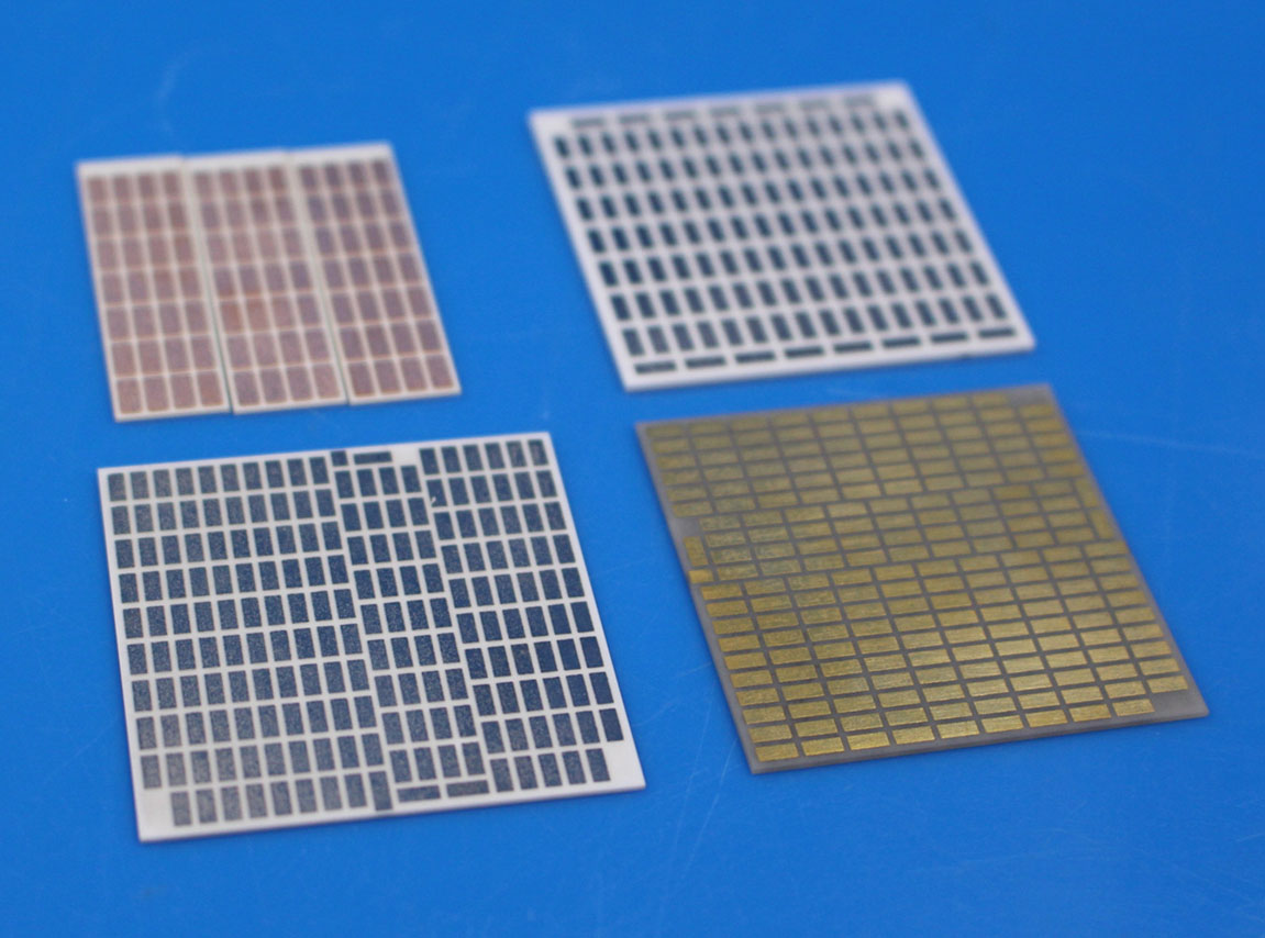
ここでは、それぞれのプロセスとその利点・欠点について解説します。
DBCは、セラミック基板、接合層、導電層から構成されます。高温下で銅箔をアルミナまたは窒化アルミニウムセラミック基板表面に直接接合する特殊なプロセスです。
メリットは以下のとおりです。
- 銅層が厚い;
- 加工が速い;
- 価格が安い;
- 多層構造が可能;
- 大面積での使用に適している;
- 高い熱伝導率;
- 高い密着強度;
- 優れた軟ろう付け性;
- 優れた電気絶縁性
デメリットは以下のとおりです。
- 穴を通過できない。
- 精度が低い。
- 平面度(表面粗さ)が低い。
- 製品から離れた位置にある装置には適しているが、精密な位置決めには適さない。
DPC(直接銅めっき)
主に蒸着、マグネトロンスパッタリングなどの表面蒸着プロセスを用いて基板表面に金属めっきを施します。まず真空下でチタン粒子を蒸着し、次に銅粒子を蒸着してめっき厚を決定し、その後通常のプリント基板(PCB)製造工程で配線を仕上げます。さらにめっき/無電解めっき法を用いて配線厚を増します。DPCの製造工程には、真空蒸着、湿式蒸着、露光現像、エッチングなどのプロセスが含まれます。
メリットは以下のとおりです。
- 形状加工に関して、DPCセラミック基板はレーザー切断が必要であり、従来のボール盤やフライス盤、パンチプレスでは高精度な加工ができないため、合力と線幅もより微細になる。
- 金属の結晶性能に優れる;
- 平面度が良好;
- 配線が剥がれにくい;
- 配線位置の精度が高く、配線間隔が狭く、信頼性と安定性に優れ、貫通孔加工などのメリットを有る。
デメリットは以下の通りです。
薄板(厚さ300μm以下)しか作製できず、コストが高く、生産量も限られているため、頻繁な出荷では納期を守れない可能性があります。
AMBは、ろう材中の少量の活性元素であるTiとZrをセラミックスと反応させ、溶融ろう材が濡れる反応層を形成することで、セラミックスと金属の接合を実現する方法です。
メリットは以下の通りです。
この組み合わせは、セラミックと活性金属はんだペーストが高温で化学反応を起こすことで実現されるため、接合強度が高く、信頼性も優れています。
デメリットは以下のとおりです。
AMBプロセスの信頼性は、活性フィラー金属の組成、ろう付けプロセス、ろう付け層の構造、その他多くの重要な要素に大きく依存します。
厚膜技術は、セラミック基板に直接印刷されたグラフィックを、直接焼結するプロセスです。
メリットは以下のとおりです。
- セラミックとの密着力がDPCプロセスよりもはるかに高い。
- エッチングや銅メッキ工程を経ずにグラフィックを直接印刷するため、コストが低くなる。
- 一度の成形で済むため、DPCよりも平滑性が優れている。
デメリットは以下のとおりです。
厚膜プロセスは印刷方式のため、一般的に厚みはそれほど厚くありません。製品の要求仕様によって、使用する材料が異なるため、フィルムの導電率に影響が出ます。
そのため、どのプロセスが最適かを一概に言うことは難しく、お客様の用途や使用状況によって異なります。お客様は、それぞれの要件に応じてプロセスを選択できます。
ご興味をお持ちいただけましたら、いつでもお気軽にお問い合わせください。
声明:これはINNOVACERA®のオリジナル記事です。転載する際は、出典リンクを明記してください:https://www.innovacera.com/ja/news-ja/process-comparison-of-the-ceramic-substrate.html。


 お問い合わせ