.svg)
The metallized ceramic substrate is a kind of circuit board. It has a thermal expansion coefficient close to that of semiconductors and high heat resistance. It is suitable for products with high heat generation (high-brightness LED, solar energy), and its excellent weather resistance is more suitable for harsh outdoor environments. Because it has the characteristics of lead-free, non-toxic, and good chemical stability, it will not cause harm to environmental protection, so it is more and more widely accepted by the public.
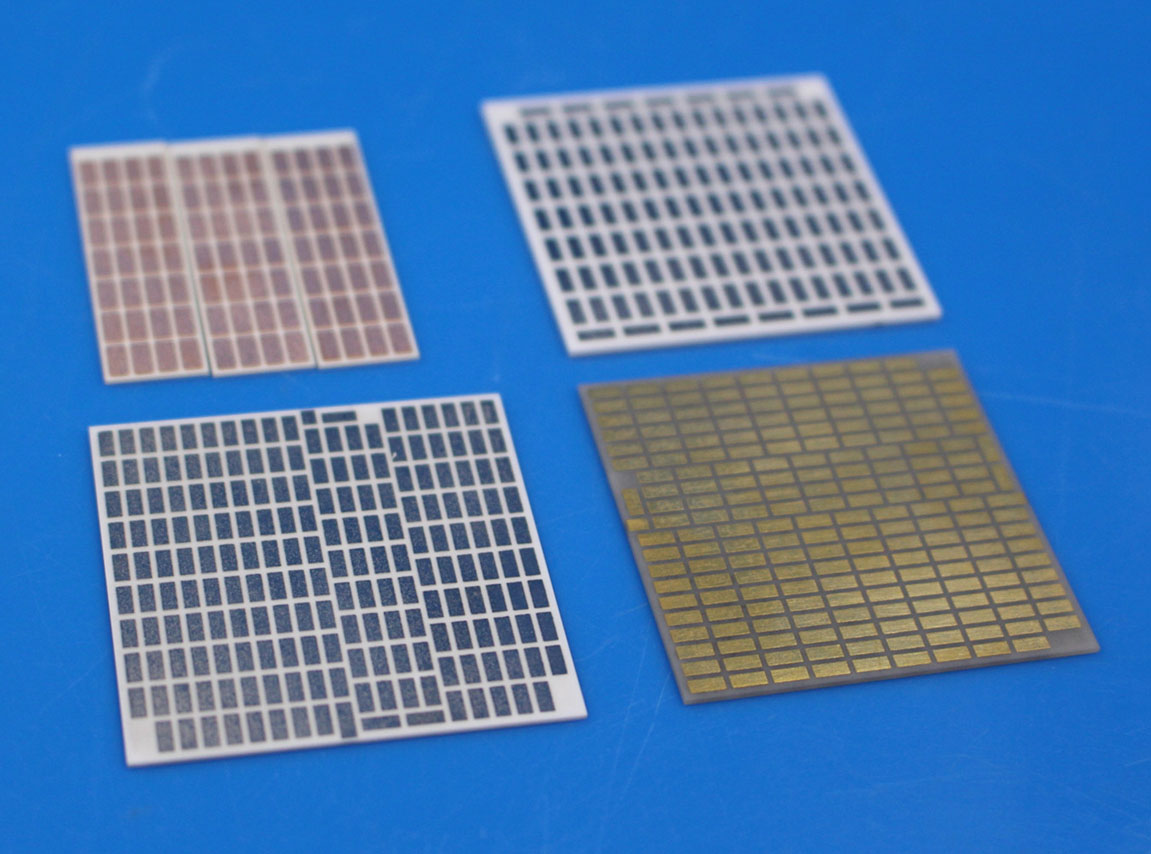
Due to different processes, the ceramic substrate is mainly divided into DBC (Direct Bonded Copper), DPC (Direct Plated Copper), AMB (Active Metal Brazing), and Thick film.
We will introduce each of the processes and the advantages, disadvantages of each process.
It is composed of the ceramic substrate, bonding layer, and conductive layer. It refers to the special process of copper foil directly bonding to alumina or aluminum nitride ceramic substrate surface at high temperature.
The advantages are as below:
- The copper layer is thick;
- The processing is fast;
- The price is cheap;
- Can make multilayer;
- Suitable for large area consumption;
- High thermal conductivity;
- High adhesion strength;
- Excellent soft brazing;
- Excellent electrical insulation
The disadvantages are as below:
- Can not pass through the hole;
- Poor accuracy;
- Low flatness (surface roughness);
- Suitable for the device in the large distance of the product, can not be done in the precise occupation.
DPC (Direct Plated Copper)
Mainly by evaporation, magnetron sputtering and other surface deposition process to carry on the substrate surface metallization, first under the condition of vacuum sputtering, titanium, and then is copper particles, the plating thickness, then finish making line with ordinary PCB craft, and then to plating/electroless deposition way to increase the thickness of the line, the preparation of DPC way contains vacuum coating, wet deposition, Exposure development, etching, and other processes.
The advantages are as below:
- In terms of shape processing, DPC ceramic plate needs to be cut by laser, the traditional drilling and milling machine, and punch machine can not be accurately processed, so the combined force and line width are also finer.
- The crystal performance of the metal is good;
- The flatness is good;
- The line is not easy to fall off;
- The line position is more accurate, the line distance is smaller, reliable, and stable, can be through the hole and other advantages.
The disadvantages are as below:
It can only make a thin plate (thickness < 300μm), and its cost is high, the output value is limited, resulting in frequent shipment time can not be on time.
It is a method to realize the bonding of ceramic and metal by reacting a small number of active elements Ti and Zr in filler metal with ceramics to form a reaction layer that can be wetted by liquid filler metal.
The advantages are as below:
The combination is achieved by the chemical reaction between ceramic and active metal solder paste at high temperatures, so its bonding strength is higher and reliability is better.
The disadvantages are as below:
The reliability of the AMB process depends largely on the composition of active filler metal, brazing process, brazing layer structure, and many other key factors.
Thick film technology is straight on ceramic substrate printed graphics, then direct sintering process.
The advantages are as below:
- The bonding force with ceramic is much greater than that of the DPC process;
- It is direct printing of graphics, no etching, and copper plating process, so the cost will be lower;
- It is a one-time forming, so the flatness is smoother than that of the DPC.
The disadvantages are as below:
Because the thick film process is printed, it is generally not too thick. Due to different product requirements, different materials have a certain impact on the conductivity of the film.
So it is hard to say which process is best, it depends on the customer’s application and usage, customer could choose each of the processes according to their requirements.
Should you have more interests, pls feel free to contact us at any time.
Declaration: This is an original article of INNOVACERA®. Please indicate the source link when reprinting: https://www.innovacera.com/news/process-comparison-of-the-ceramic-substrate.html.


 Enquiry