.svg)
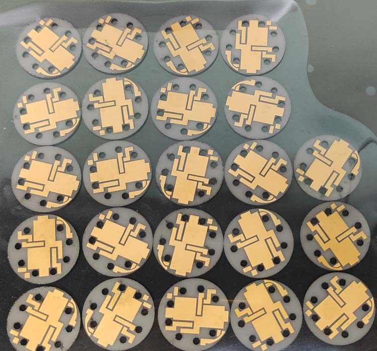
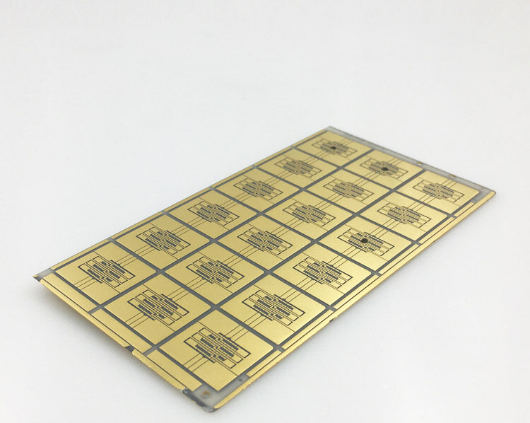
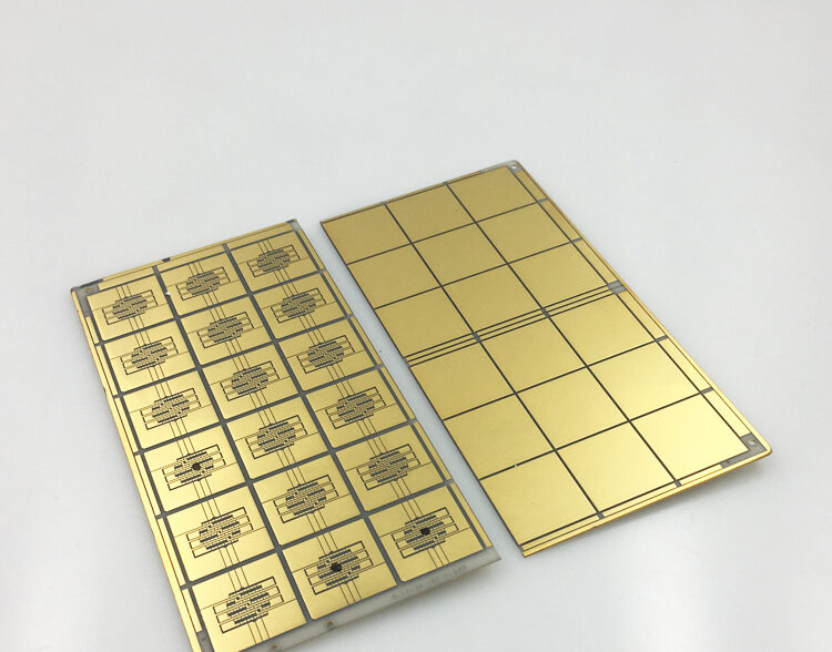
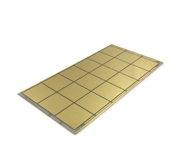
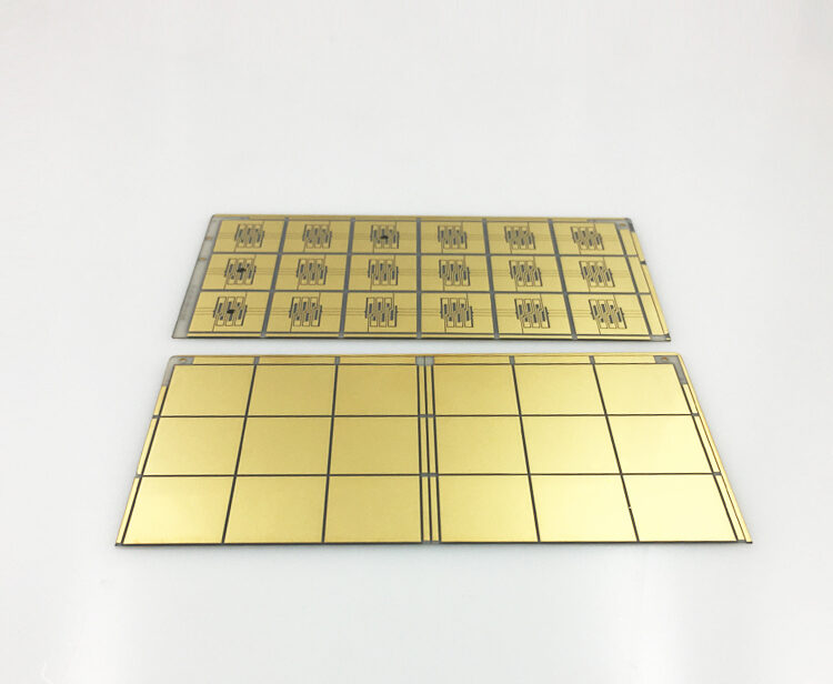
Direct Plated Copper Substrate Key Attributes :
– Superior CTE and excellent thermal conductivity
– High reliability and durability
– Good Mechanically performance
– Low electrical resistance conductor traces
– Superior high-frequency characteristics
– Fine line resolution
– Low temperature process (below 300℃) guarantee the quality of ceramic and the metallized layer, also reduce the cost.
Direct Plated Copper Substrate Applications:
– High Power LED Packaging
– Hybrid and electric automobile power management electronics
– RF microwave communication
– Substrates for solar concentrator cells
– Power semiconductor packaging
– Laser system
– Fiber laser pump
DBC vs DPC
DBC being suited to high current capacity, however limited on circuit design. DPC allowing for finer tracks and through hole connection.
Declaration: This is an original article of INNOVACERA®. Please indicate the source link when reprinting: https://www.innovacera.com/product/direct-plated-copper-substrate.
 Enquiry