.svg)

Material Properties
| Property | Value | 92F | 93D | |
| Color | – | – | Black | White |
| Al2O3 Content | – | % | 92 | 93 |
| Density | 25℃ | g/cm3 | 3.7 | 3.65 |
| Thermal Conductivity | 25℃ | W/(m· K) | 20 | 18 |
| Coefficient of Linear Thermal Expansion | 40℃~400℃ | x10-6/℃ | 6.7 | 7 |
| 40℃~800℃ | 6.9 | 7.2 | ||
| Volume Resistance | 20℃ | Ω·cm | 1014 | 1014 |
| 300℃ | 1010 | 1010 | ||
| 500℃ | 108 | 109 | ||
| Dielectric Constant | 1MHZ | – | 10 | 9 |
| Dielectric Loss | 1MHZ | x10-4 | 4 | 4 |
| Flexural Strength | 0.5mm/min | MPa | 400 | 400 |
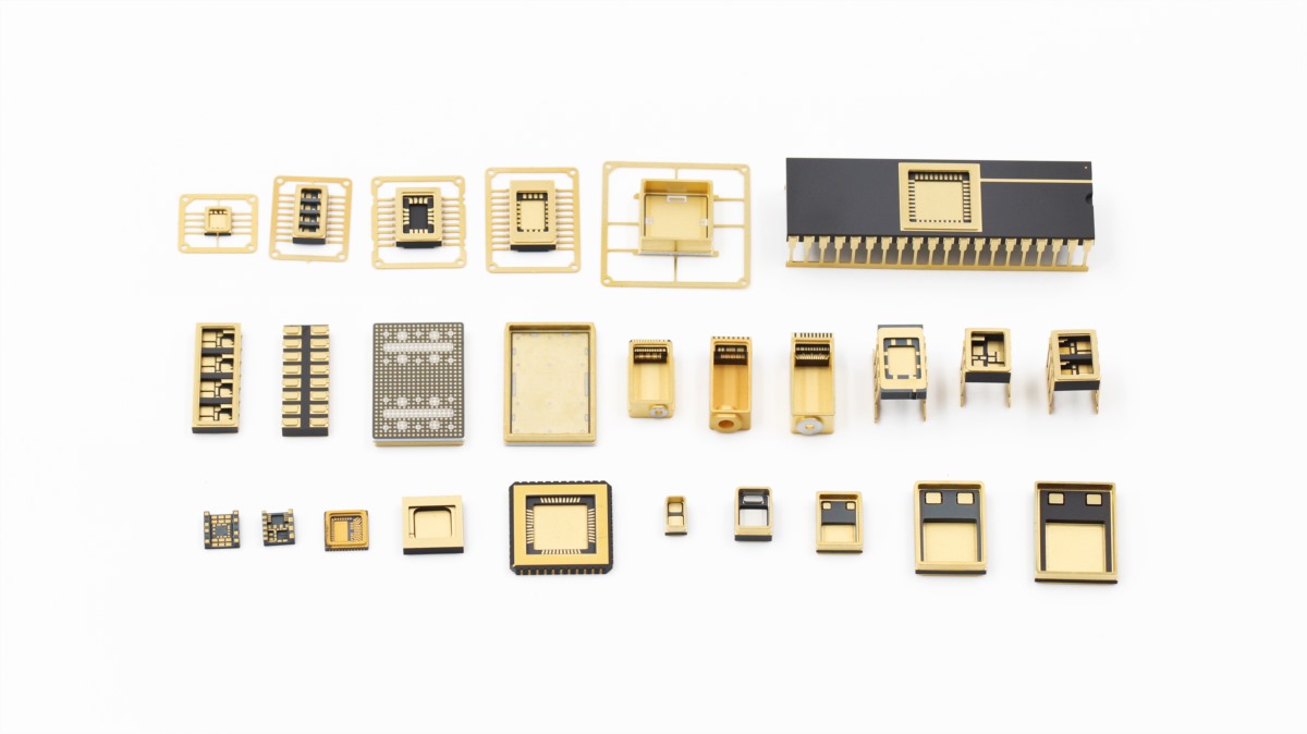
Ceramic packaging shells come in various structural forms depending on the characteristics and operating environments of different devices.
1. Ceramic Small Outline Package (CSOP)
Features:
- Compact size, wing-shaped leads, low stress
- Excellent resistance to mechanical shock
- Multiple lead pitches: 1.27mm, 1.00mm, 0.80mm, etc.
Applications:
- IC packaging
- High-reliability component packaging for space, radiation, or military/defense applications
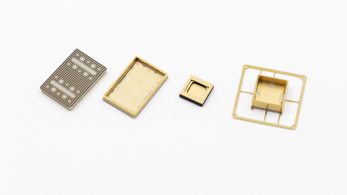
2. Surface-Mount Device package (SMD)
Features
- High electrical conductivity and current-carrying capacity
- Large-area heat sink for the chip bonding zone
- Reliable performance and excellent thermal dissipation
Applications:
- Microwave device housing
- Crystal oscillator housing
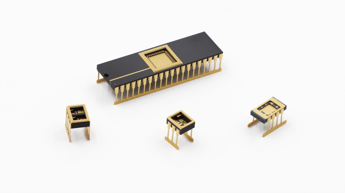
3. Ceramic Dual in-line Package (CDIP)
Features
- Dual in-line package
- Wide range of pin counts
- EMI/RFI Protection
Applications:
- Programmable Logic Device, LSI
- Optocouplers, MEMS devices, etc.
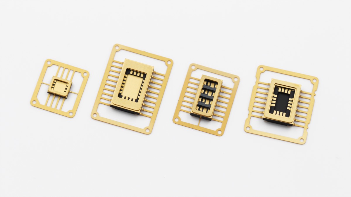
4. Ceramic Leadless Chip Carrier/Ceramic Quad Flat Non-leaded Package (CLCC/CQFN)
Features
- Low parasitic parameters and compact size
- Excellent heat dissipation and high reliability
- Available in dual-sided and quad-sided lead configurations
- Multiple lead pitches: 1.27mm, 1.00mm, 0.50mm, etc.
Applications:
- Suitable for high-density surface mounting
- VLSI, ASIC, and ECL circuits
5. Laser SMD package
Features
- High thermal conductivity, superior crystal protection
- Stable performance and driving power
- Compact surface-mount device 7mm combined with built-in safety
- Enables ultra-long projection distances, narrow beam angles, and compact optical sizes
Applications:
- Portable Search and Rescue Lighting
- Automotive and Construction Lighting
- Outdoor and entertainment Lighting
6. ROSA/TOSA package
Features
- High airtightness and reliability
- Meets speed requirements from 10 GHz to 400 GHz in various applications
- Customizable development available
Applications:
- Fiber optic communications
- Optoelectronic transmitters and receivers
- Optical switches and modules, High-power lasers
Innovacera offers one-stop ceramic packaging solutions, ranging from standard parts to fully customized designs. For ceramic package housings, please feel free to contact us.
Declaration: This is an original article of INNOVACERA®. Please indicate the source link when reprinting: https://www.innovacera.com/product/ceramic-packages.
 Enquiry