.svg)
Today, with 5G communication base station power amplifiers facing heat dissipation bottlenecks, new energy vehicle electric drive control units needing to operate stably in high-temperature environments (up to 150℃ or higher), and satellite payload electronic equipment having to endure extreme temperature cycles, traditional plastic packaging technology is encountering unprecedented performance challenges. It is precisely against this backdrop that CLCC (Ceramic Leadless Chip Carrier) / CQFN (Ceramic Quad Flat No-leads) Ceramic Quad No-Lead Packages, with their outstanding heat dissipation capabilities, excellent high-frequency characteristics are becoming the preferred solution for high-end electronic system design.
Technical Definitions and Core Characteristics
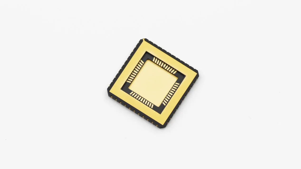
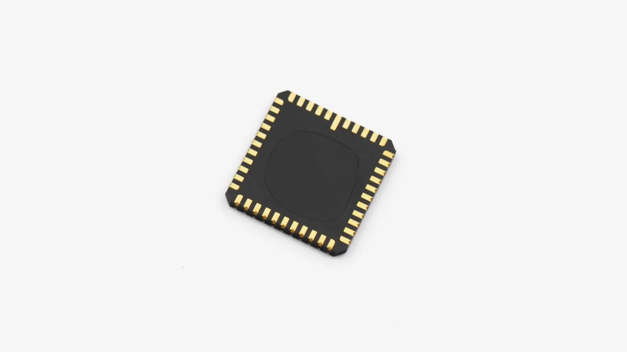
CLCC and CQFN both belong to the four-sided leadless surface mount packaging manufactured on a high thermal conductivity ceramic substrate. Both are assembled using metallized solder terminals arranged on all four sides. However, their structural designs have different focuses, tailored to suit different application scenarios.
CLCC is a standardized ceramic chip carrier with a cavity. Its structure is primarily designed to provide a reliable and sealed protective environment for the internal chips, suitable for IC packaging with extremely high requirements for long-term stability. The chips can be interconnected through upward gold wire bonding in the cavity or through flip-chip bonding in the cavity.
The CQFN is a type of package that, without using lead wires, integrates a key feature: a large-area bare heat dissipation pad at the bottom. This design is aimed at establishing an efficient heat path for chips (especially power devices), enabling them to maintain the advantages of four-sided mounting while significantly outperforming the standard CLCC in terms of heat dissipation performance.
Compared with traditional plastic packaging, this type of packaging has the following characteristics:
●High-reliability ceramic material: Using aluminium oxide (Al2O3) or aluminium nitride (AlN), they are resistant to high temperatures, corrosion and aging, and remain stable in extreme environments for a long time.
●Four-sided leadless design: The pads are distributed on the bottom or around, supporting SMT (Surface Mount Technology), high-density PCB layout, and occupying a small space.
●Excellent electrical performance and heat dissipation: Ceramic materials are naturally insulating and have high thermal conductivity, which effectively dissipates heat and ensures the stable operation of high-frequency and high-power devices.
●Precision fabrication process: Powder forming, precise sintering, surface metallization, uniform size, flat pads, suitable for high-precision surface mount and welding.
●High dependability: The metallized solder joints are closely bonded to the ceramic substrate, and can operate stably for a long time in high-temperature, high-humidity and vibration environments.
●Various lead structures: Support dual-side and quad-side packaging.
●Multiple lead pitch options: Available in 2.7 mm, 1.00 mm, and 0.50 mm, meeting diverse design requirements.
Application scenarios:
CLCC/CQFN ceramic packaging is an ideal carrier for high-end integrated circuits suitable for surface mount technology (SMT). It is specifically designed for packaging chips that have strict requirements for performance and stability, such as:
(1) Various very-large-scale integrated circuits (VLSI)
(2) Special Application Integrated Circuit (ASIC)
(3) High-speed emitter-coupled logic (ECL) circuits
Due to its outstanding technical capabilities, CLCC/CQFN has become a key solution in numerous high-end electronic systems.
Typical applications include:
5G Communication Infrastructure: For base station power amplifiers (such as GaN/LDMOS devices), to meet the stringent heat dissipation requirements under high-frequency, high-speed operation.
New energy vehicle electric drive system: Used for the motor control unit (MCU) and power module, it ensures the system can operate stably for a long time under high power and high-temperature conditions.
Aerospace and Satellite Payloads: Carrying the core processing and signal chain circuits, ensuring that the equipment can withstand extreme temperature cycles, vacuum environments and high-intensity vibrations.
In short, the CLCC/CQFN ceramic quad flat no-leads package combines the high reliability of ceramics with the convenience of modern surface mount packaging, making it an ideal choice for high-end electronic system design.
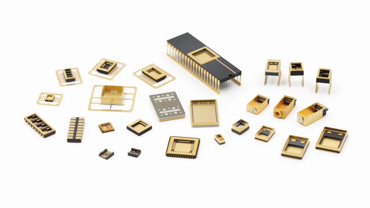
In addition to the ceramic quad no-leads package (CLCC/CQFN), Innovacera also offers a wide range of ceramic packaging options, including:
Surface-Mount Ceramic Power Package
Optical Communication Device Enclosures(ROSA/TOSA)
Ceramic Dual In-Line Package (DIP) Enclosure
Ceramic Small Outline Package
These products can meet the requirements of various application scenarios and provide customers with comprehensive and highly reliable solutions. Innovacera has now officially launched several ceramic packaging enclosure. Please feel free to contact us to obtain technical materials, samples, or customized solutions. Let’s jointly explore more possibilities in the design of high-end electronic systems.
Declaration: This is an original article of INNOVACERA®. Please indicate the source link when reprinting: https://www.innovacera.com/news/clcc-cqfn-high-reliability-ceramic-packages-driving-high-end-electronics.html.

 Enclosure")
")
 Enquiry