Ceramic packaging stands out as the material of choice for optical communication, power devices and aerospace systems, and automotive electronics, thanks to its exceptional thermal performance, excellent dielectric properties, and hermetic sealing capability. Unlike plastic packages, ceramic solutions excel in high-temperature and harsh environments, as well as applications demanding long service life and high reliability. Moreover, ceramic package housings can be tailored into a variety of structural forms to perfectly match the specific characteristics and operating conditions of different devices.
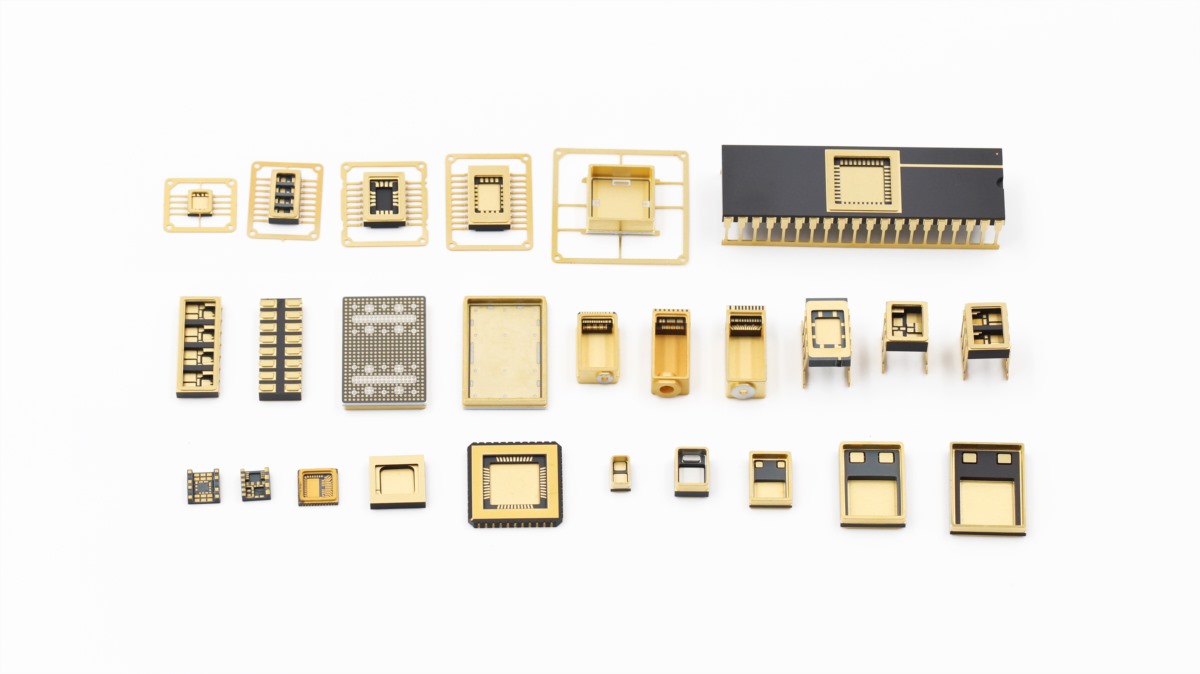
The following sections introduce several representative product series:
1. Ceramic Small Outline Package (CSOP)
The CSOP (Ceramic Small Outline Package) is a commonly used miniature surface-mount package. Its leads extend from both sides, with pitch options including 1.27 mm, 1.00 mm, and 0.80 mm. CSOP offers advantages such as low manufacturing cost, excellent performance, high reliability, compact size, light weight, and high packaging density.
Features:
Miniaturized design with gull-wing leads, minimizing stress
Excellent resistance to mechanical shock
Multiple lead pitches available: 1.27 mm, 1.00 mm, 0.80 mm
Applications:
Various integrated circuits, high-reliability component packaging
2. Ceramic Surface-Mount Power Package (SMD)
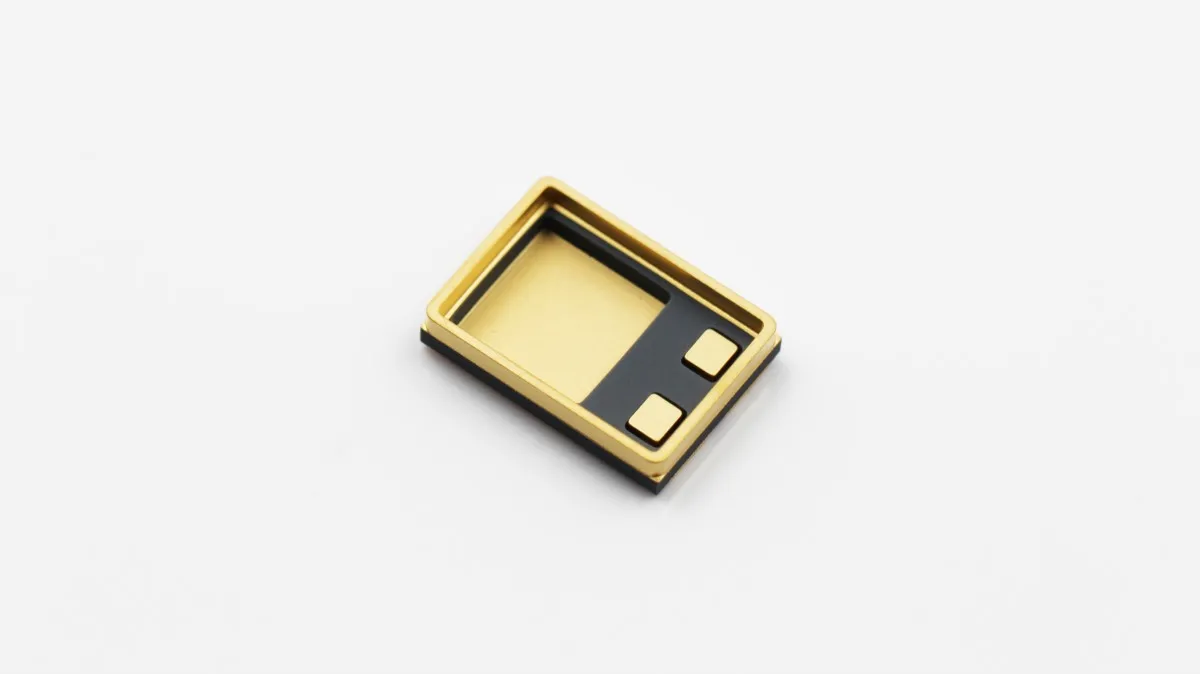
Designed for power devices and high-heat-flux components—such as power semiconductors, resistors, and power ICs—the ceramic SMD package provides extremely low thermal resistance pathways and excellent thermal contact surfaces, allowing heat to be rapidly conducted to the PCB or heatsink.
Features:
High current-carrying capability
Large chip bonding area serving as an efficient heat sink
Reliable performance with superior thermal management
Applications:
Microwave device housings
Crystal and oscillator device packages
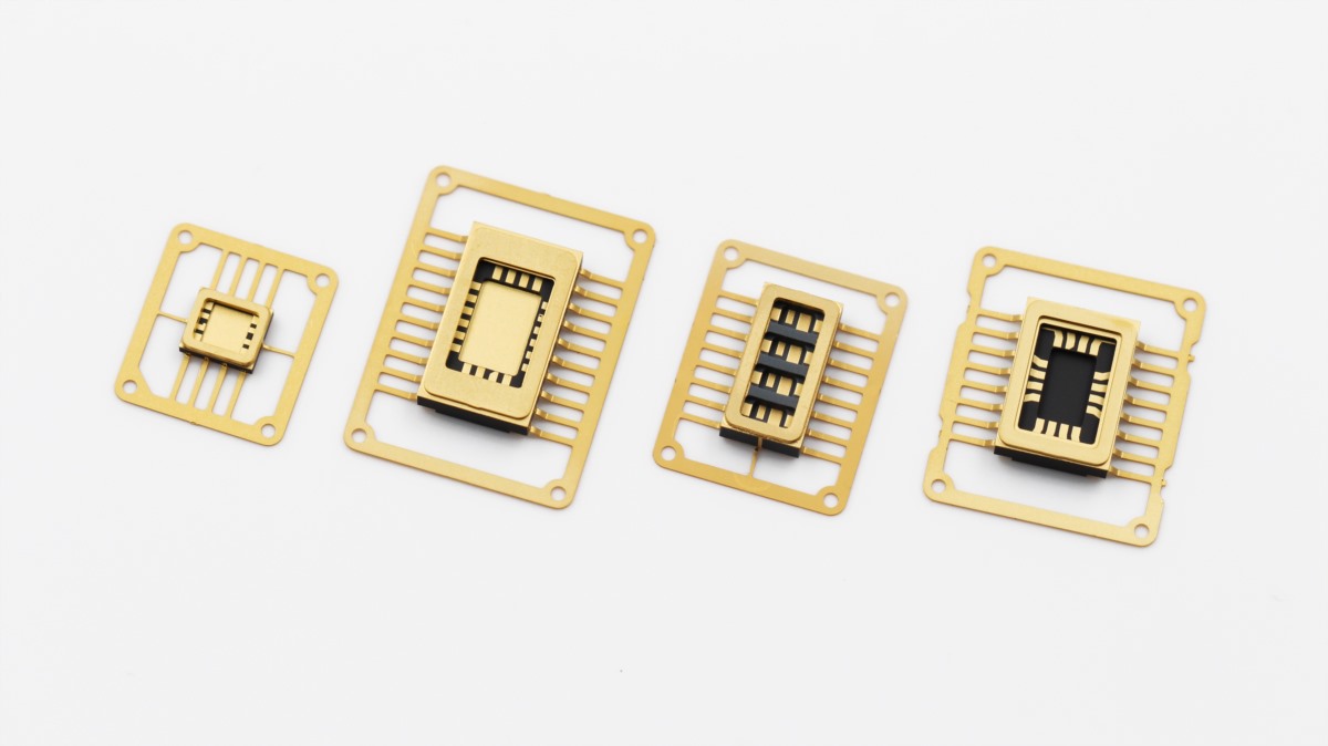
3. Ceramic Dual In-line Package (CDIP)
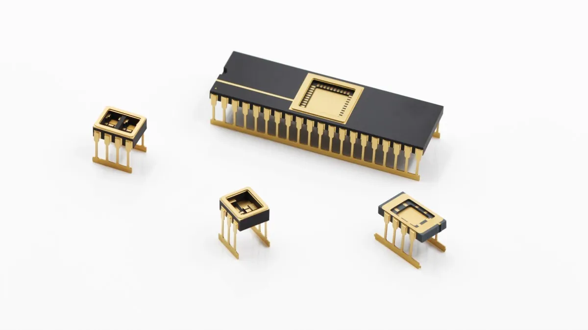
The CDIP (Ceramic Dual In-line Package) is one of the most widely used through-hole packages. It consists of two pressed ceramic blocks enclosing a dual in-line lead frame, with leads extending from both sides of the package. Standard lead pitches are typically 2.54 mm, and the number of leads ranges from 6 to 64. CDIPs offer excellent thermoelectric performance and high reliability.
Features:
Dual in-line lead configuration
Wide range of lead counts
Applications:
Various integrated circuits with moderate pin-out and assembly density requirements
Optocouplers, MEMS devices, and other high-reliability components
4. Ceramic Leadless Quad Packages (CLCC / CQFN)
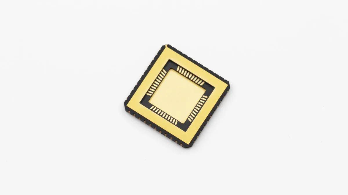
CLCC (Ceramic Leadless Chip Carrier) and CQFN (Ceramic Quad Flat No-leads) belong to the leadless or no-exposed-lead quad package family. They are ideal for high-frequency, low-parasitic inductance applications that require efficient thermal dissipation and high-reliability integrated circuit packaging.
Features:
Low parasitic parameters with compact size
Excellent thermal management and high reliability
Available in dual-side or four-side lead configurations
Multiple lead pitch options: 1.27 mm, 1.00 mm, 0.50 mm, etc.
Applications:
High-density surface-mount applications
Various VLSI, ASIC, and ECL circuits
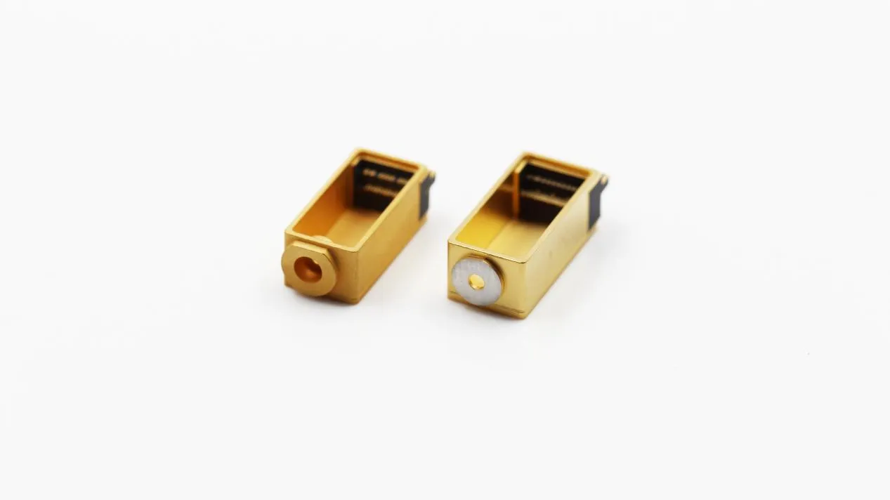
5. Laser SMD Ceramic Packages
The core function of laser device ceramic packages is optical control. Their purpose is to safely encapsulate a light-emitting or light-receiving chip while efficiently and reliably transmitting optical signals to the outside, and effectively managing the heat generated. Proper thermal management in laser packages ensures a stable, optimal operating temperature, thereby maintaining wavelength stability and consistent output power.
Features:
High thermal conductivity with excellent chip protection
Stable performance and reliable driving capability
Compact 7 mm surface-mount design with built-in safety features
Enables long projection distances, narrow beam angles, and small optical dimensions
Applications:
Portable exploration and rescue lighting
Automotive and architectural lighting
Outdoor and entertainment lighting
6. Optical Communication Package Series (ROSA / TOSA, etc.)
ROSA (Receiver Optical Sub-Assembly) and TOSA (Transmitter Optical Sub-Assembly) are critical submodule packages in optical device modules (such as SFP/QSFP) that house key optoelectronic components—including laser diodes, photodiodes, and fiber coupling windows. Ceramic ROSA/TOSA packages are commonly used in applications requiring high frequency, high-speed operation, excellent thermal management, and hermetic window sealing.
Features:
High hermeticity with extremely low leakage, ensuring a stable internal optical environment
Excellent thermal management for extended service life
Supports a wide range of data rates from 10 GHz to 400 GHz
Customizable design to meet specific user requirements
Applications:
Fiber-optic communication systems
Various optoelectronic transmitter and receiver devices
Optical switches, modules, and high-power laser systems
Innovacera offers a one-stop ceramic packaging solution, ranging from standard components to fully customized designs. From material selection, ceramic processing, metallization, and sealing, to hermeticity and reliability testing, we work closely with customers to develop prototypes and scale up to mass production.
Declaration: This is an original article of INNOVACERA®. Please indicate the source link when reprinting: https://www.innovacera.com/news/complete-ceramic-housing-solutions-for-optical-communication-and-electronic-packaging.html.


 Enquiry