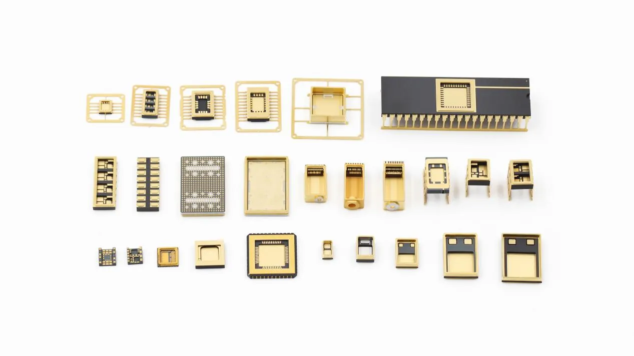
In the modern electronics industry, the three types of ceramic packaging and component technologies, namely HTCC, LTCC and MLCC, jointly form the foundation of high-performance electronic systems.
Although they all belong to the multi-layer ceramic technology system, their application directions and performance emphases are different:
HTCC is used for high-reliability and high-power packaging, LTCC excels in integrating high-frequency and multi-functional circuits, and MLCC is the core type of surface-mount passive components.
These three factors jointly support the high performance and miniaturization development of modern electronic devices.
This article mainly introduces the HTCC packaging technology:

HTCC packaging combines alumina or aluminum nitride porcelain wafers with tungsten/molybdenum metal circuits through a set of precision ceramic-metal co-firing process, and finally forms a high-density, highly reliable three-dimensional ceramic circuit structure through key steps such as molding, printing, co-firing and packaging.
The key steps include:
(1) Ceramic substrate preparation (tape casting):
Mix the ceramic powder (such as alumina) with organic binders, plasticizers and solvents to form a uniform slurry. Then, use a casting machine to shape it into a certain thickness of raw porcelain sheet.
This step requires strict control of drying conditions and slurry viscosity to ensure uniform thickness and flat surface of the raw film, providing a stable foundation for subsequent printing and lamination.
(2) Circuit Printing:
Conductive lines and through-holes are formed on the surface of the raw porcelain pieces through the screen printing process. Using tungsten, molybdenum or their alloys as the metal conductor enables it to withstand the subsequent high-temperature co-firing process.
After printing, it is usually dried and degreased at low temperature to ensure that the metal circuit is firmly adhered to, the pattern is clear, and there are no bubbles and impurities.
(3) Layering and Lamination:
The printed multi-layer preforms are precisely aligned and overlapped, and the interlayer bonding is achieved through heat pressing or isostatic pressing techniques to form a three-dimensional interconnection structure.
The accuracy of this step directly affects the size tolerance of the finished product and the reliability of conduction.
(4) High-temperature co-firing:
In a reducing atmosphere, the ceramics and metal conductors are sintered together at a temperature of around 1600℃ to achieve synchronous densification, thereby forming a robust multi-layer substrate.
The finished product usually undergoes a volume contraction of approximately 15—20%, so compensation for this shrinkage needs to be taken into account during the design stage.
(5) Post-processing techniques:
Carry out processing such as metallization, electroplating, cutting, welding, pin installation or gas sealing on the sintered substrate.
Some of the high-end HTCC products will also undergo solder pre-coating, electrode strengthening or laser marking to meet the demanding requirements of medical or high-temperature electronic applications.
Technical Advantages
· Excellent high-temperature stability
The HTCC package can operate stably for a long time in an environment of 300–350°C.
With special design, it can even withstand short-term extreme high temperatures above 400°C.
Its ceramic framework maintains structural integrity and airtightness at high temperatures, which is crucial for achieving high-temperature electronic packaging.
· Outstanding electrical insulation property
The ceramic matrix itself is an excellent insulating material, featuring low dielectric constant and low dielectric loss, which helps ensure the integrity of high-frequency signal transmission and reduces interference.
· High mechanical strength and environmental durability
The structure is sturdy and can withstand thermal shock, mechanical vibration and corrosive environments.
Its reliability is much higher than that of ordinary plastic packaging and it is suitable for use in harsh conditions such as industrial and aerospace applications.
· Support high-density three-dimensional integration
By stacking multiple layers of porcelain tiles and achieving vertical interconnection, a complex three-dimensional wiring structure can be realized, supporting high pin count, high frequency and miniaturized packaging designs.
· Excellent thermal management performance
Ceramic materials (especially aluminum nitride, AlN) have a high thermal conductivity, which can effectively transfer the heat generated by the chip, thereby increasing the power density and service life of the device.
Application Fields
· Automotive electronics: Applied in engine control modules (ECU), pressure sensors and on-board power modules to cope with the high temperatures and vibrations within the engine compartment.
· Industry and Energy: Provides services for core power conversion equipment such as frequency converters and inverter power supplies, ensuring their long-term operation under high temperatures and high power densities.
· High-frequency communication: As the RF circuit and filter carrier in 5G base stations and radar systems, it ensures the low-loss transmission of high-frequency signals.
· Sensor technology: Provides sturdy and airtight packaging shells for various MEMS, gas, infrared and pressure sensors, suitable for harsh conditions.
· High-end equipment: It is the key packaging solution for highly reliable control systems in aerospace, and implantable medical devices.
Thus, whether it is to cope with harsh environmental challenges or to achieve the ultimate performance, HTCC ceramic packages offers a proven and reliable path.
When your project is subjected to demanding conditions such as high temperature, high frequency, high power or long-term reliability, HTCC might just be the key solution.
INNOVACERA is dedicated to providing customers with professional HTCC ceramic packaging solutions. Please feel free to contact us.
Declaration: This is an original article of INNOVACERA®. Please indicate the source link when reprinting: https://www.innovacera.com/news/htcc-ceramic-packaging-technology-the-key-to-high-power-and-high-frequency-applications.html.


 Enquiry