01
Power Electronics
Ceramic substrates are widely used in power modules, IGBT modules, DC-DC converters and other power electronic devices for excellent heat dissipation performance, high insulation and long-term reliability.
VIEW MORE +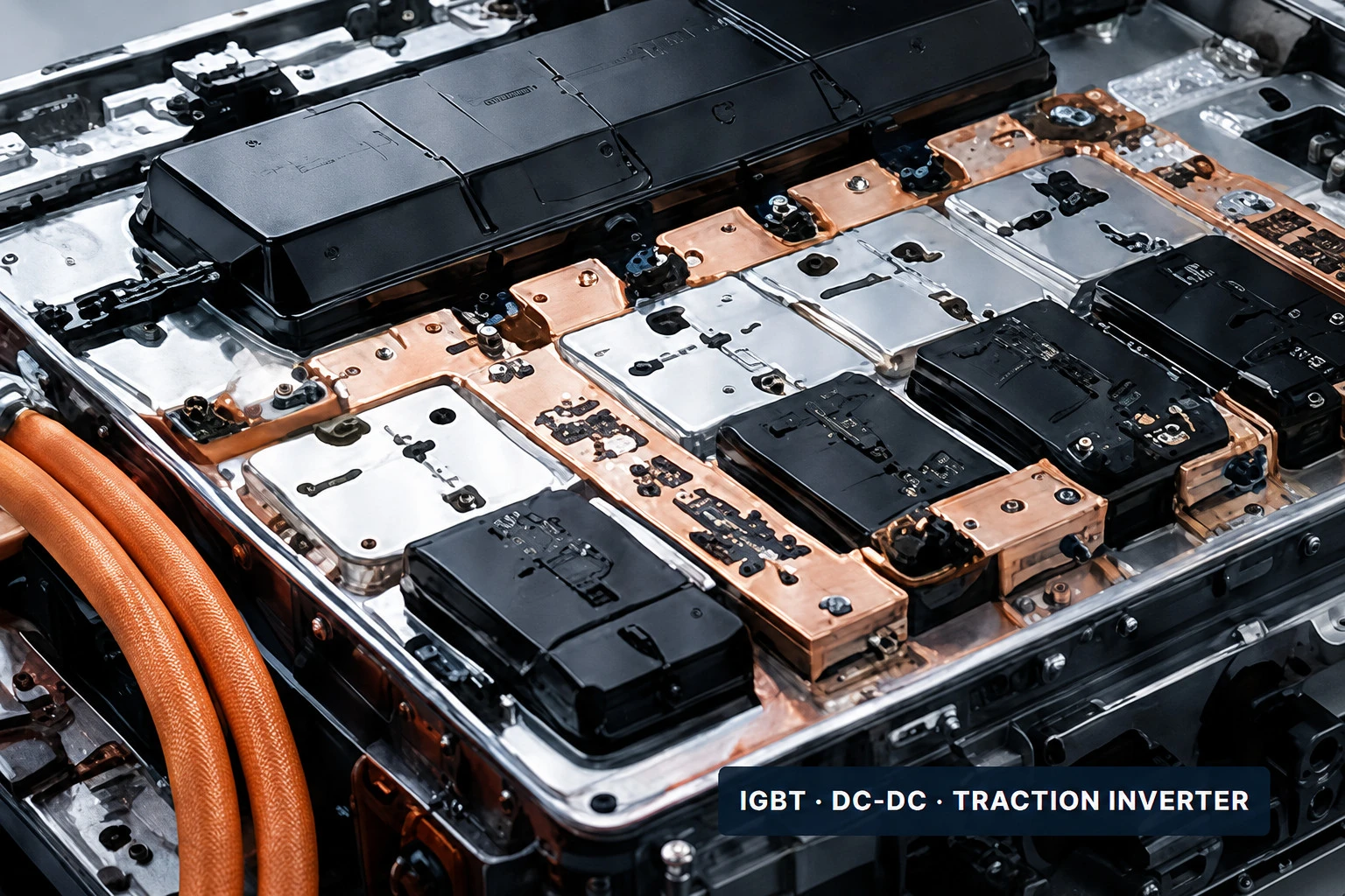

Built for demanding electronic assemblies, ceramic substrates create a reliable platform for power, signal, and thermal management. From compact modules to high-density circuits, they help engineers achieve more performance in less space.
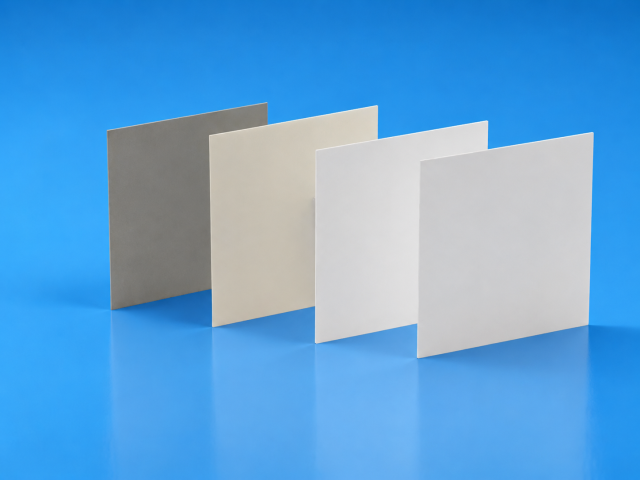

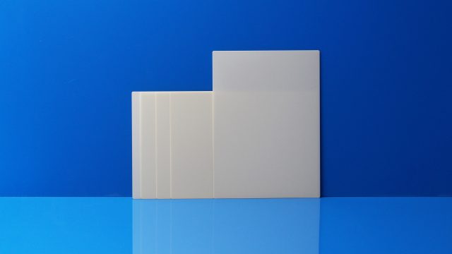
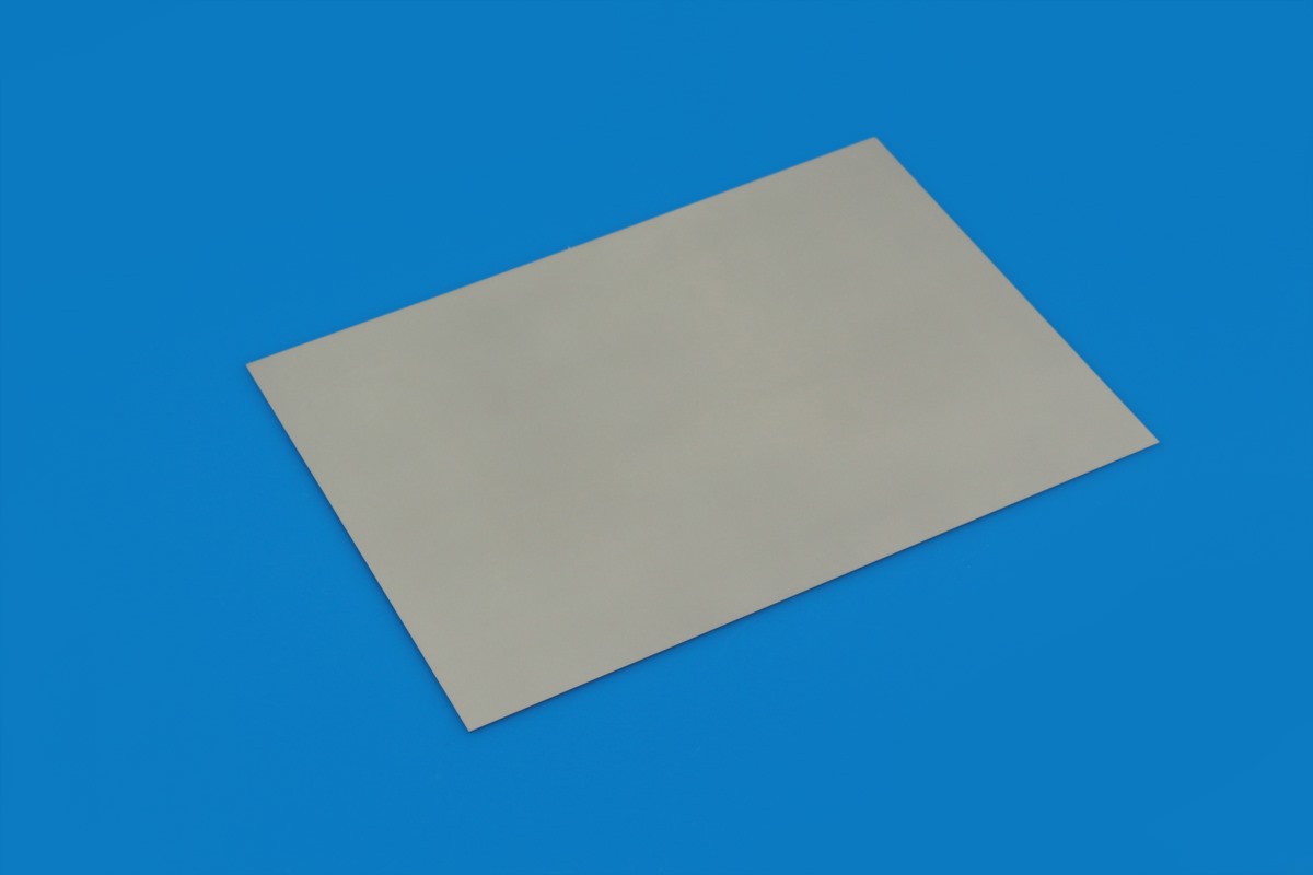
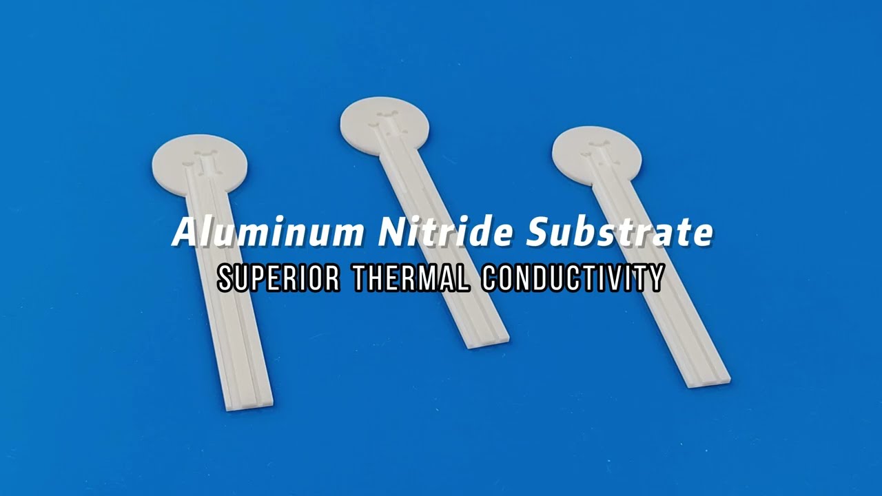
Ceramic substrates provide electrical insulation, thermal management, dimensional stability and a reliable base for metallized circuits across power electronics, LED lighting, semiconductor packaging and high-frequency communication systems.
Ceramic substrates are widely used in power modules, IGBT modules, DC-DC converters and other power electronic devices for excellent heat dissipation performance, high insulation and long-term reliability.
VIEW MORE +
Ceramic substrates with high thermal conductivity provide an ideal heat dissipation solution for high-power LED chips, improving luminous efficiency and extending the service life of LED products.

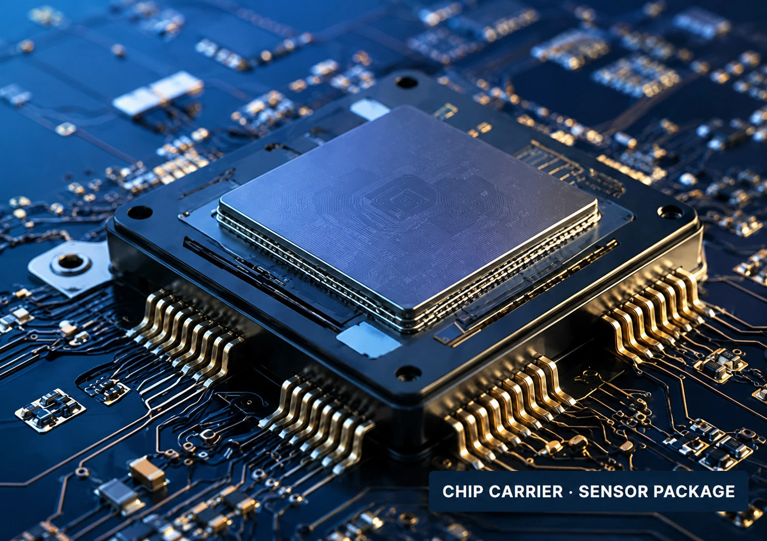
Used for chip carriers, sensor packages and other semiconductor packaging applications, ceramic substrates offer excellent flatness, dimensional stability and compatibility for high-density integration.
Low dielectric loss and stable dielectric constant make ceramic substrates ideal for RF/microwave modules, filters, antennas and communication devices, ensuring signal transmission stability at high frequencies.

View product demonstrations covering AlN and alumina substrates, DPC metallization and AMB substrate technology for power, LED and semiconductor applications.
These answers cover material selection, metallization, customization and the technical information needed to review a ceramic substrate project.
Alumina is widely selected for dependable electrical insulation and cost-effective circuit support. Aluminum nitride is preferred when higher thermal conductivity and a thermal expansion match closer to silicon are important. Silicon nitride is considered for high mechanical strength and demanding thermal-cycling conditions. Final selection should be based on heat load, voltage, mechanical stress, dimensions and cost target.
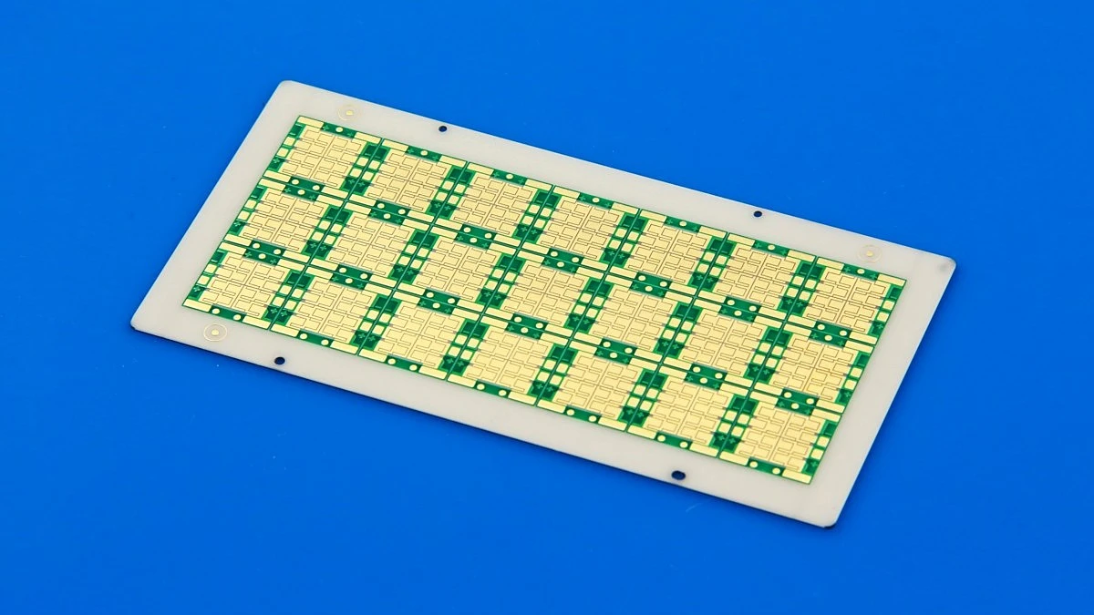
DBC bonds relatively thick copper to alumina, AlN or other suitable ceramics and is commonly used where high current and strong heat spreading are required. DPC uses sputtering, photolithography and copper plating to create finer conductor patterns, thinner copper layers and through-hole connections for compact or high-density electronic packages.
Yes. Custom dimensions, thicknesses, holes, slots, edge profiles, surface roughness, flatness, polishing and metallization layouts can be reviewed according to the drawing and application requirements.
Depending on the material, circuit geometry and assembly method, options may include thick-film and thin-film metallization, direct bonded copper, direct plated copper, active metal brazing and other customized conductor or plating systems.
Yes. Ceramic substrates are widely used where electrical isolation, heat transfer, high-frequency performance, dimensional stability or reliable metal-to-ceramic integration is required. The substrate material and metallization route should be matched to current, voltage, thermal load, frequency and package design.
Provide the drawing or Gerber data, substrate material, thermal conductivity target, dimensions, thickness, flatness, surface finish, copper or metallization specification, plating finish, electrical and thermal operating conditions, quantity and project stage.
Innovacera supports ceramic substrate projects from material and process selection through precision machining, metallization, sampling and repeat production for electronic and semiconductor applications.
Alumina, AlN, silicon nitride and metallization routes can be reviewed against thermal, electrical, mechanical and cost requirements.
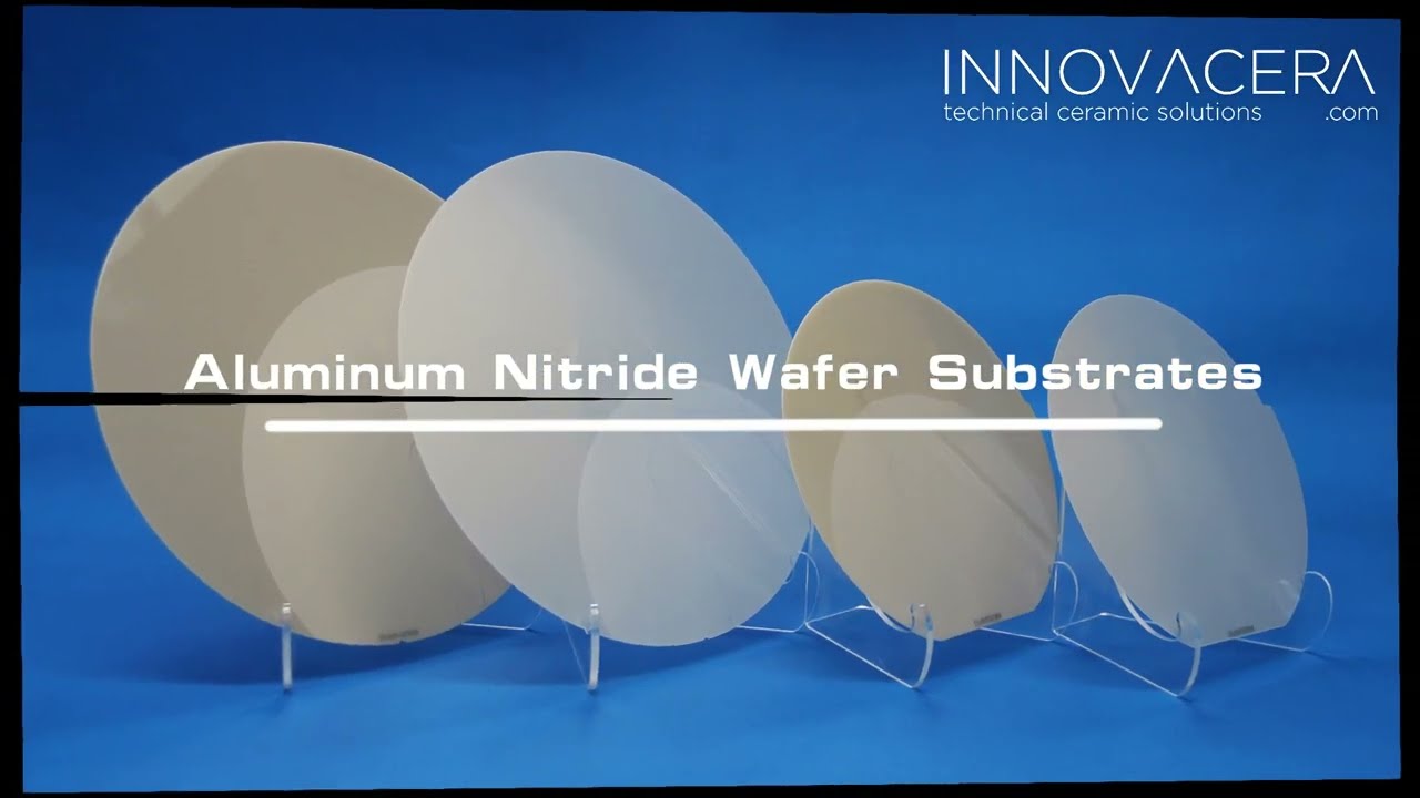
Support for custom thickness, flatness, polished or lapped surfaces, holes, slots, contours and wafer-style geometries.
Circuit pattern, copper thickness, plating finish, solderability and ceramic-to-metal interfaces can be reviewed as one assembly requirement.
Engineering samples and prototype validation can be followed by controlled repeat supply after specifications are confirmed.
To recommend a suitable ceramic material and manufacturing route, please provide the substrate geometry, thermal and electrical requirements, surface condition, metallization design and expected quantity.
For metallized substrates, Gerber data or a clearly dimensioned conductor drawing will help review line width, spacing, copper thickness, via design, edge clearance and plating finish.
Submit Ceramic Substrate RFQSend drawings, operating conditions, material preference, tolerance targets and quantity. Innovacera can review standard catalog products or custom ceramic manufacturing paths.