Alumina Oxide is one of the most cost-effective and widely used substrate materials in microelectronic applications. While many customers will be satisfied with an as-fired surface for their applications, there are four major benefits of ceramic substrate polishing:
- Finer Line Patterns
After the fine grinding and polishing process, the ceramic substrate can get finer pattern lines, which is beneficial to the denser circuit design ability and is conducive to fine-pitch, high-density interconnection circuits.
An as-fired surface finish is generally adequate for lines as thin as 1 mil in thin-film applications and 5 mils in thick-film applications. Forming finer lines than these on as-fired surfaces will exhibit poor pattern definition resulting in increased conductor resistance, which inhibits current flow and reduces circuit performance. Poor pattern definition can also contribute to performance anomalies in RF and microwave circuits, so we will polish it.
- Better Top and Bottom Surface Parallelism
Grinding and polishing the substrate can improves the parallelism between the top and bottom surfaces. The benefit is that the capacitance and inductance of the substrate can be more tightly controlled when the substrate is metalized and patterned. Since capacitance and inductance are the main factors determining impedance, increased parallelism can improve the predictability and performance of RF and microwave circuits.
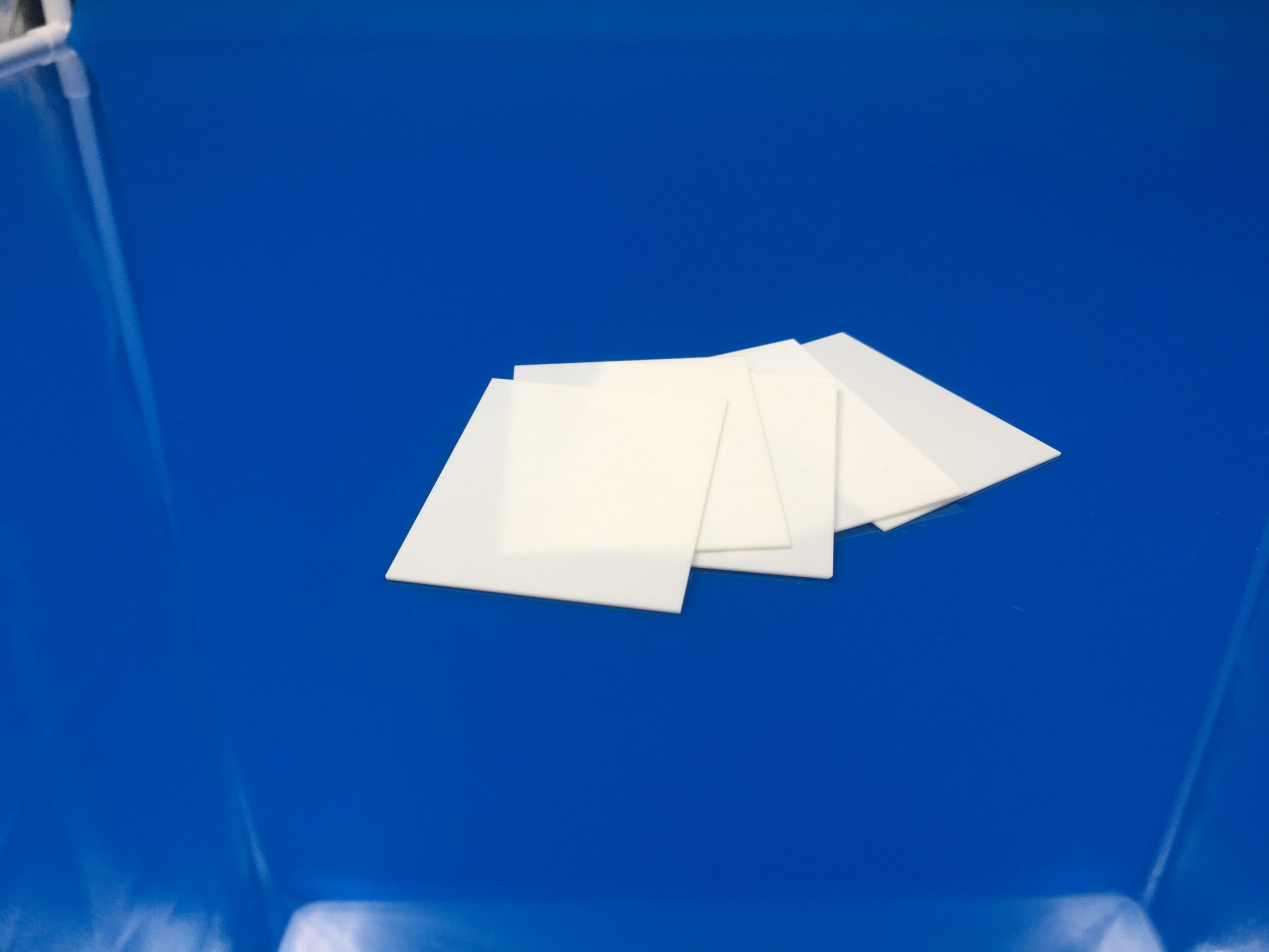
99.6% Alumina Polishing Ceramic Substrates
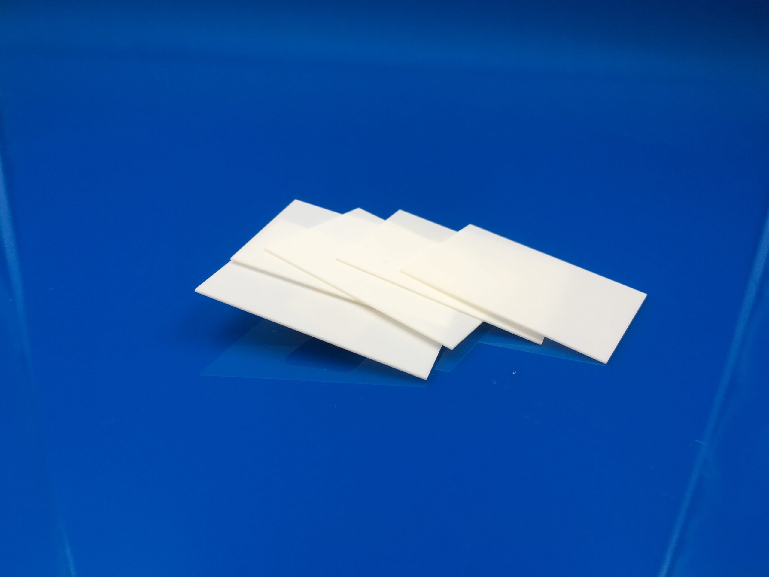
Why Polish Ceramic Substrates
- Thinner Metallization Layers
Polishing reduces the amplitude of peaks and valleys on the substrate surface enabling the use of significantly thinner metalization layers. Thinner resistive layers increase the sheet resistance of the material, which allows for higher resistance values when using thin-film technology—especially when using serpentine patterns.
- Better Optical Performance
The very nature of fabricated optical devices demands surface smoothness and flatness beyond that typically required by microelectronics. Generally, light must be precisely moved around, bent reflected, split, sent through fibers, and used in ways that were not intended by nature. All of this has to be accomplished with as little loss of light as possible. In most cases, the colors can’t be altered or shifted within the spectrum. Polishing and super polishing are the only means that can achieve highly reflective or transmissive surfaces. The surface must be polished and flattened to a small fraction of a wavelength for optimum performance.
Declaration: This is an original article of INNOVACERA®. Please indicate the source link when reprinting: https://www.innovacera.com/news/why-polish-ceramic-substrates.html.


 Enquiry