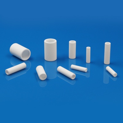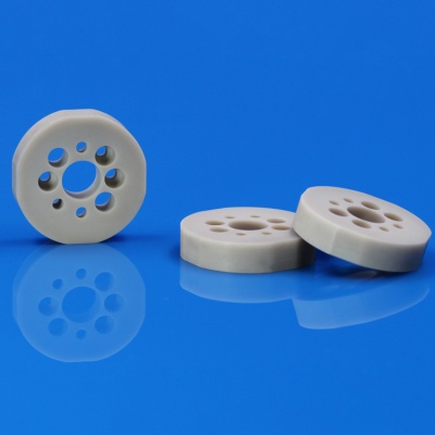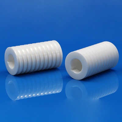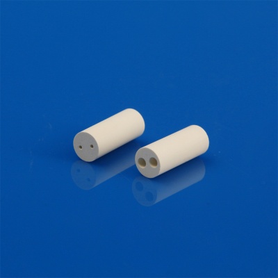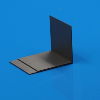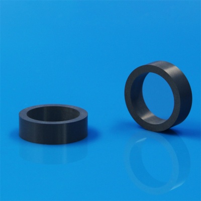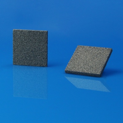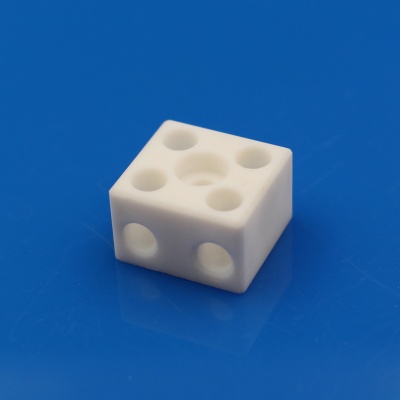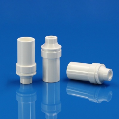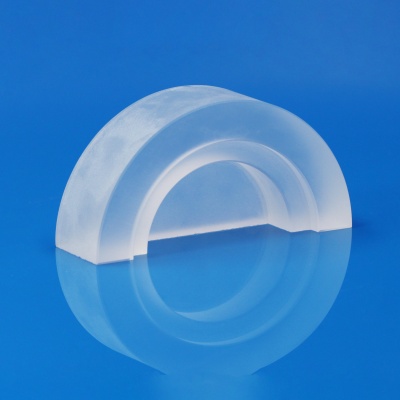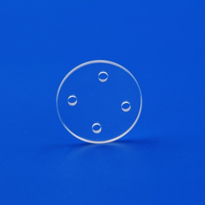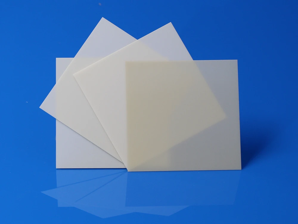
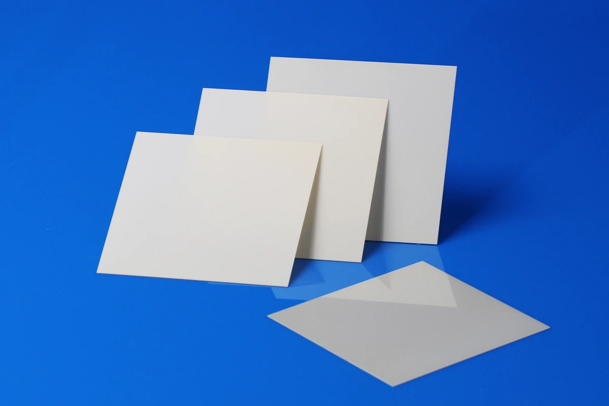
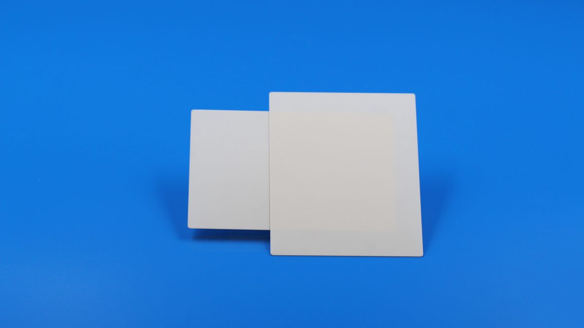
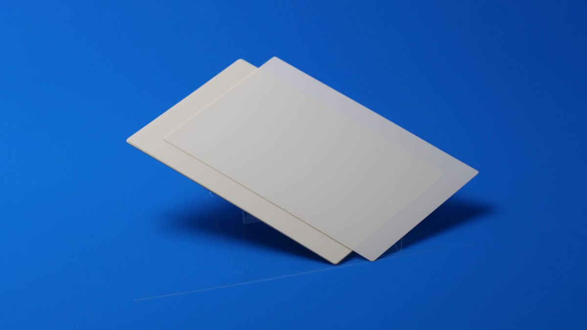
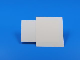
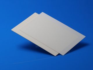
230 W/m·K high thermal conductivity aluminum nitride substrates are widely used in laser and photonic applications, because its efficient heat transfer and electrical insulation are essential for compact electronic and optoelectronic assemblies where concentrated heat loads demand higher thermal conductivity. AlN can be used as a mounting substrate or submount between the laser diode and the package or heat sink. INNOVACERA supplies standard or custom sizes 230 W/m·K aluminum nitride substrates, grinding, polishing and precision machining process is available.
230 W/m·K aluminum nitride substrates test samples data
A 100 × 100 × 0.55 mm sample achieved an average thermal conductivity of 231 W/(m·K).
| Parameter | Value |
|---|---|
| Thermal Conductivity | ≥230 W/(m·K) |
| Average Measured Value | 231 W/(m·K) |
| Flexural Strength | 392 MPa |
| Density | 3.28 g/cm³ |
| Test Sample Size | 100 × 100 × 0.55 mm |
The values above are representative test data for the sample tested.
For applications requiring a finer surface finish, the substrate can be polished to Ra ≤0.05 μm.
Common Sizes
| Size | Thickness |
|---|---|
| 100 × 100 mm | 0.38 / 0.55 / 0.635 mm |
| 114.3 × 114.3 mm | 0.38 / 0.55 / 0.635 mm |
| 120 × 120 mm | 0.38 / 0.55 / 0.635 mm |
Custom sizes and thicknesses can also be evaluated according to your drawing.
Typical Applications
The 230 W/m·K grade is mainly intended for applications where heat dissipation is a critical design requirement.
Typical applications include:
- AlN laser diode submounts
- High-power laser modules
- Laser diode arrays
- Photonic and optoelectronic components
- Optical communication modules
- High-power semiconductor devices
- Other compact thermal management assemblies
For an AlN substrate for laser diode packaging, surface finish, dimensions and tolerances can be customized according to the mounting and assembly requirements.
Precision Processing
Available processing options include:
- Polishing to Ra ≤0.05 μm
- Surface grinding
- Precision cutting
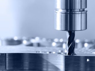
- Laser machining
- Holes and slots
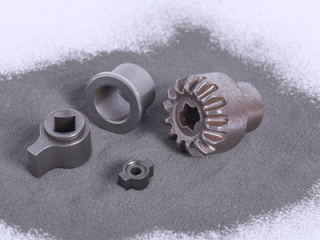
- Custom shapes and dimensions
For laser diode, photonic or other precision applications, please send your drawing together with the required size, thickness, surface finish and tolerances.
Declaration: This is an original article of INNOVACERA®. Please indicate the source link when reprinting: https://www.innovacera.com/product/230-wmk-aluminum-nitride-substrates
Frequently Asked Questions
Why Are 230 W/m·K AlN Substrates Vital for Laser Diodes? How Do They Prevent Thermal Roll-Over?
High-power semiconductor lasers generate intense localized heat flux that causes emission wavelength drift, threshold current increases, and catastrophic optical mirror damage (thermal roll-over). INNOVACERA’s 230 W/m·K aluminum nitride (AlN) substrates provide superior thermal dissipation alongside high dielectric insulation. Functioning as heat-spreading submounts between the laser die and copper package, their thermal expansion coefficient closely matches GaAs and InP chips, eliminating thermal mismatch stress and dramatically lowering junction temperatures.
Need Mirror Polishing or Laser Micro-Dicing for Photonic Packages? How to Order Custom AlN Wafers from INNOVACERA?
Laser diode packaging requires ultra-flat, mirror-polished submounts for void-free eutectic die bonding. INNOVACERA provides full custom precision processing for 230 W/m·K AlN substrates, supporting double-sided polishing down to Ra <= 0.05 µm, laser profiling, micro-via drilling, and custom dicing. In addition to standard formats (100x100 mm, 114.3x114.3 mm, 120x120 mm) and thicknesses (0.38, 0.55, 0.635 mm), customers can request bespoke dimensions and metallization pads tailored to their optoelectronic module designs.