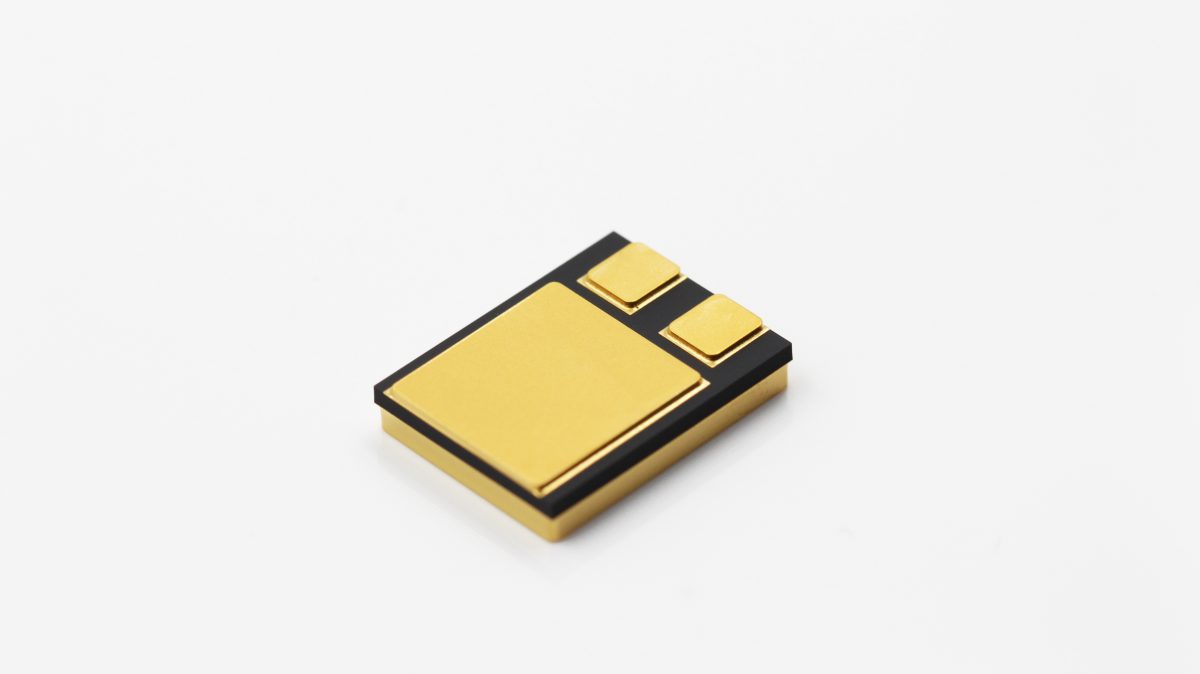
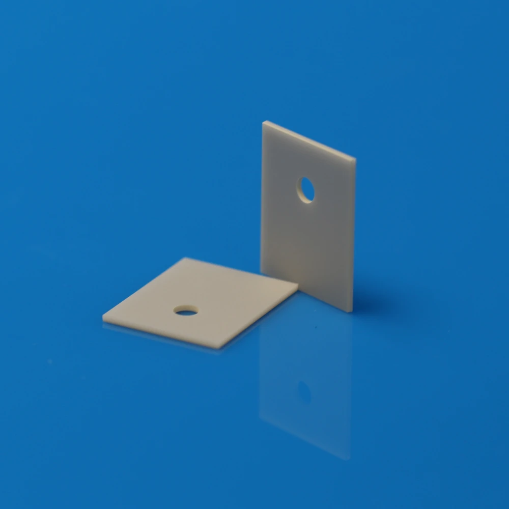
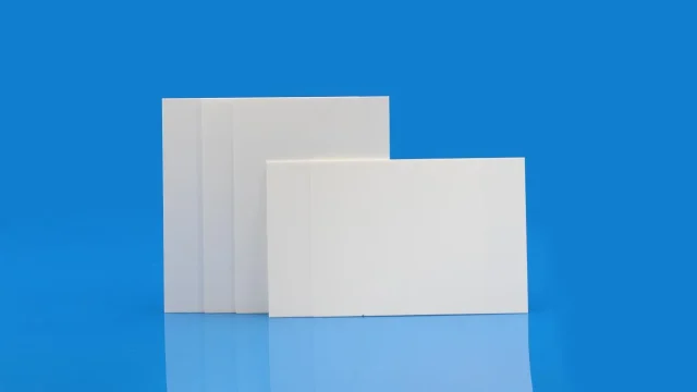
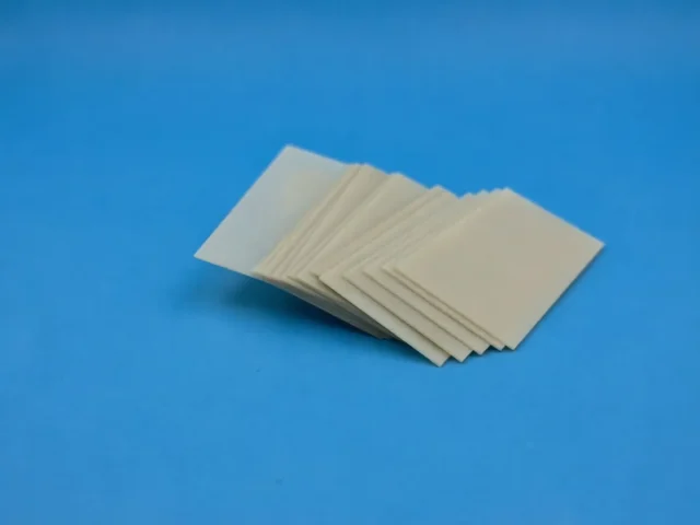
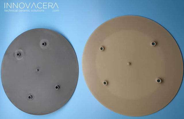
In the engineering design of aluminum nitride ceramic substrates, 0.635 mm and 1.0 mm are the two most common structural thickness options, widely used in front-end metallization processes such as DPC, DBC, and AMB. For the standard platform size of 138 × 190 mm (typically serving as the base material for subsequent dicing), the choice of thickness not only affects thermal performance but also directly determines the stability boundary of the structure during thermal cycling and assembly.
In practical projects, a typical yet often overlooked issue is:
Even when thermal design requirements are met, packaging structures still exhibit warpage amplification, interfacial delamination, or failure during thermal cycling in later stages.
Such problems are usually not caused by insufficient material properties, but rather by a mismatch between the selected thickness and the system’s stress pathways.
1. How Thickness Affects Thermal Path and Structural Rigidity
From an engineering perspective, the thickness of AlN substrates simultaneously influences both thermal conduction pathways and structural rigidity.
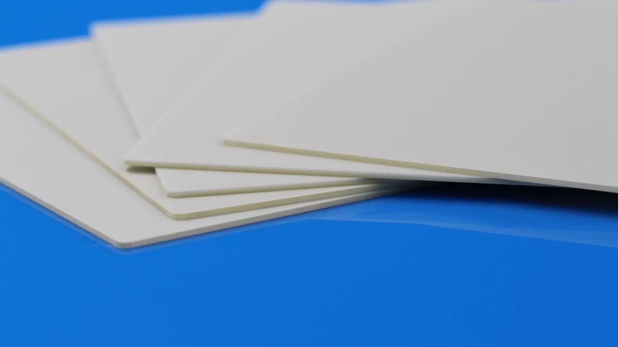
A thinner 0.635 mm substrate shortens heat transfer routes. It delivers quicker thermal response, ideal for tightly packed, miniaturized power assemblies. On the downside, thinner plates lack stiffness; they easily warp under uneven bonding forces and residual stress from metal layers.
A 1.0 mm thick substrate offers much stronger mechanical performance. It hardly deforms during manufacturing, bonding steps and repeated heating cycles, and handles varying interface stress well. Its downside is slower heat spreading, which delays thermal response when temperature spikes suddenly.
Thus, the difference between the two essentially reflects different priorities in system design.
2. Typical Manifestations of System-level Failures
During the actual DPC/DBC import process, such differences do not usually manifest directly as material failure but rather as system-level issues, such as local delamination, uneven coating stress, or structural deformation amplification after thermal cycling.
The common feature of these phenomena is that although the material inspection parameters are normal, the system behavior is abnormal.
The fundamental reason usually lies in the lack of a complete definition of the following process inputs when selecting the thickness:
• Thickness of metallization structure (copper layer or multi-layer stack)
• Bonding pressure and tooling method
• Temperature range and frequency of thermal cycling
• Density and distribution of graphic structure
• Tolerable warpage and deformation tolerance window
When these parameters are not clearly constrained, selecting based solely on thickness often cannot ensure the final system stability.
3. Engineering Compatibility Boundaries of 0.635 mm and 1.0 mm
In practical applications, the choice of these two thicknesses typically corresponds to different system design priorities.
0.635 mm is more suitable for structural designs that emphasize thermal response efficiency and high integration density, while 1.0 mm is more suitable for application environments that emphasize long-term reliability and structural stability. On a 138 × 190 mm large-sized platform, this difference will be further magnified because the size effect will enhance warping and stress accumulation behavior.
4. Engineering Selection Suggestions
Before entering the mass production design or sample verification stage, it is recommended to evaluate the thickness selection in conjunction with the actual process conditions rather than making a judgment based solely on it as an independent variable.
Generally, it is necessary to simultaneously clarify the following information:
• Metalization process path (DPC/DBC/AMB)
• Copper layer or structure layer thickness design
• Adhesion pressure and tooling method
• Thermal cycling conditions and reliability requirements
• Graphic structure density and design rules
These parameters jointly determine the reasonable range for thickness selection, rather than being determined solely by the material specifications.
Innovacera provides aluminum nitride substrate supplies and inquiry support.
Innovacera can offer large-sized AlN ceramic substrates with dimensions of 138 × 190 mm, covering common thickness specifications such as 0.635 mm and 1.0 mm. These substrates can be used for the initial base material applications in DPC, DBC, AMB and other subsequent precision processing technologies.
The products support material selection and specification matching for different application scenarios, and are suitable for various structural designs and process development requirements.
If you need selection suggestions or inquiry support, you can contact us via sales@innovacera.com.