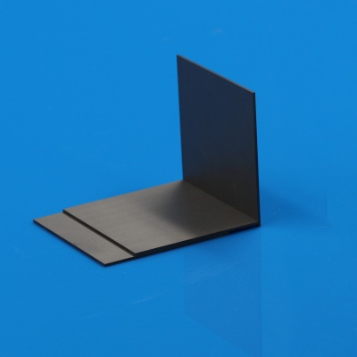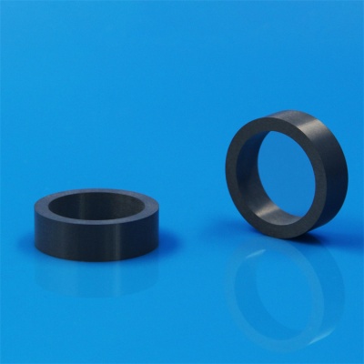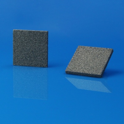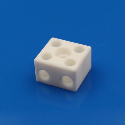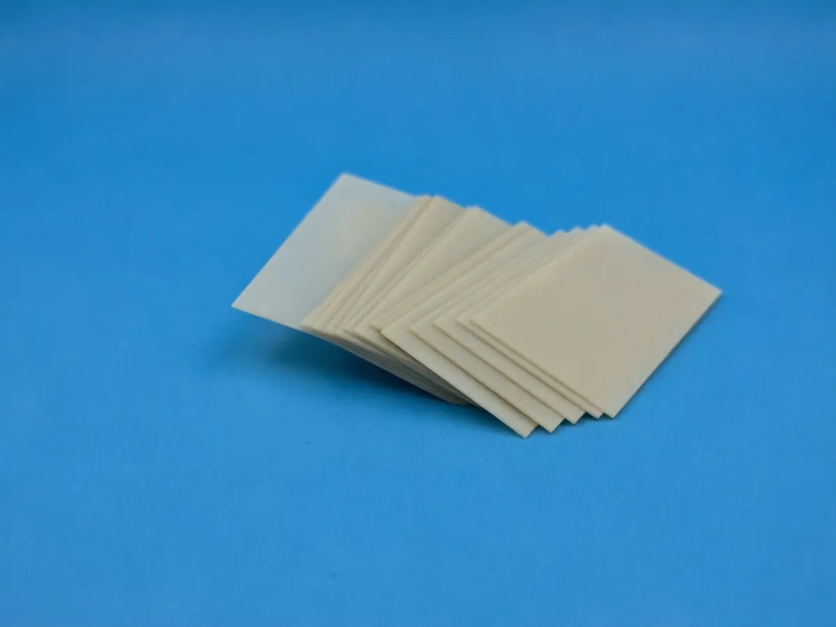
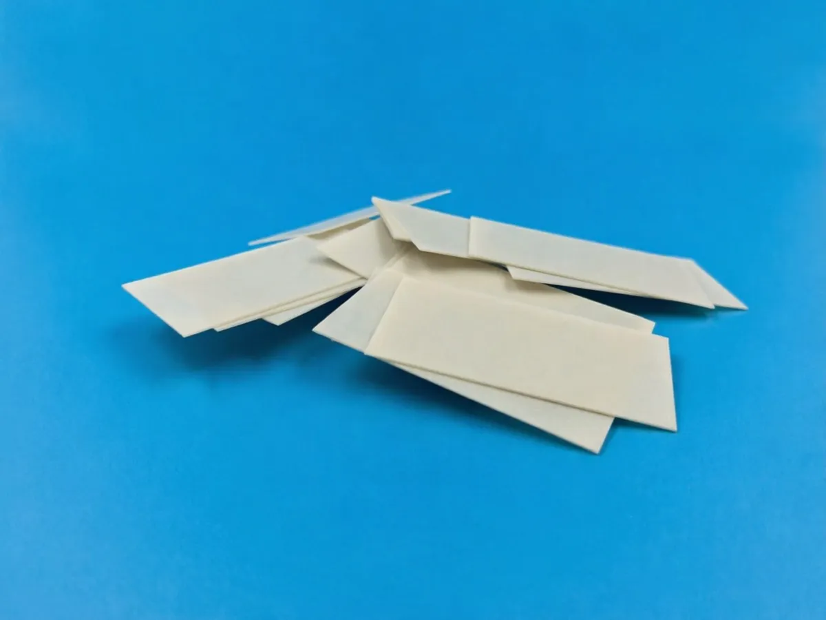
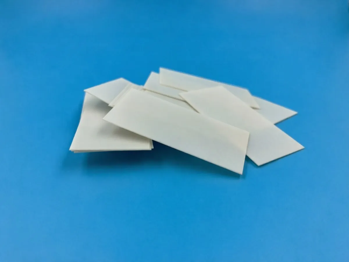
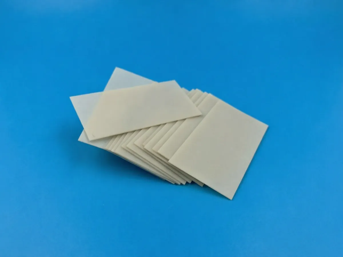
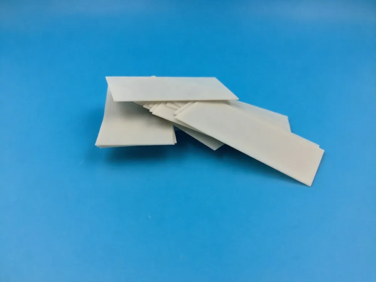

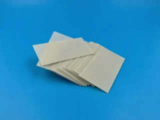
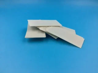
INNOVACERA provides precision-ground AlN ceramic substrates with controlled surface quality and dimensional stability for electronic packaging and downstream circuit processing. The substrates can be prepared according to different surface and processing requirements, supporting thin-film and thick-film metallization, DPC (Direct Plated Copper), AMB (Active Metal Brazing), chip mounting and other packaging processes.
Advantages:
| Feature | Technical Value |
| Controlled Surface Finish | Precision-ground surfaces with typical roughness of Ra ≤ 0.5 μm provide a suitable base for metallization, circuit processing, chip mounting and electronic packaging. |
| High Thermal Conductivity | Thermal conductivity reaches 170–230 W/m·K, supporting efficient heat transfer in electronic packages while maintaining electrical insulation. |
| Matched CTE | CTE is approximately 4.5 ppm/°C, providing a relatively close thermal expansion match with semiconductor materials and helping reduce thermally induced stress during operation. |
| Electrical Insulation | AlN ceramic combines high thermal conductivity with electrical insulation, making it suitable for electronic assemblies where heat must be transferred through an electrically insulating substrate. |
| Metallization Compatibility | Substrates can be prepared for downstream processes including thin-film metallization, thick-film metallization, DPC and AMB according to circuit and packaging requirements. |
Product Specifications & Selection
We offer three standard specifications with a thickness of 1.0 mm. Custom dimensions, thicknesses and surface requirements are also available according to drawings and downstream processing needs.
| Model | Dimensions (L×W) | Thickness | Supply Option |
| Model A | 37 × 26 mm | 1.0 mm | Standard AlN ceramic substrate for electronic packaging and subsequent processing. |
| Model B | 35 × 22 mm | 1.0 mm | Standard AlN ceramic substrate suitable for precision circuit and packaging applications. |
| Model C | 25 × 20 mm | 1.0 mm | Compact AlN ceramic substrate for space-constrained electronic assemblies. |
| Custom | According to drawing | According to requirement | Dimensions and surface conditions can be customized for specific downstream processes. |
Metallization & Downstream Processing:
1. Thin-Film Metallization
* Application Value: Precision AlN ceramic substrates provide a controlled ceramic surface for subsequent metal deposition and fine circuit patterning.
* Processing Consideration: Surface roughness, flatness and dimensional tolerance should be matched to the required thin-film structure and bonding process.
2. Thick-Film Metallization
* Application Value: AlN substrates can be used as ceramic bases for printed conductive, resistive or other functional circuit layers.
* Processing Consideration: Substrate surface condition and dimensional requirements should be confirmed according to the printing, firing and assembly process.
3. DPC Circuit Processing
* Application Value: AlN ceramic substrates combine electrical insulation and thermal conductivity, making them suitable ceramic bases for DPC circuit structures.
* Processing Consideration: Flatness, surface quality, substrate thickness and dimensions should be selected according to the circuit layout and packaging structure.
4. AMB Applications
* Application Value: AlN ceramic substrates can be used as ceramic base materials for downstream AMB copper-bonding processes in power electronic assemblies.
* Processing Consideration: Substrate dimensions, thickness and material requirements should be selected according to the copper structure, module design and operating conditions.
Electronic Packaging Applications:
AlN ceramic substrates are used in electronic packaging applications where thermal management, electrical insulation and dimensional stability are required.
1. Power Semiconductor Packaging
* Used as electrically insulating and thermally conductive ceramic bases for power semiconductor assemblies, including IGBT, MOSFET and SiC device packaging.
2. Optoelectronic Packaging
* Suitable for laser diode, photodetector and other optoelectronic packages requiring heat dissipation, stable dimensions and controlled substrate surfaces.
3. RF & Microwave Packaging
* Low dielectric loss and electrical insulation make AlN ceramic substrates suitable for high-frequency electronic assemblies and metallized circuit structures.
4. High-Power Electronic Devices
* Used in compact electronic packages where heat must be transferred efficiently while maintaining electrical isolation between the device and surrounding structure.
Why Choose Us?
INNOVACERA provides AlN ceramic substrates with standard and customized dimensions, precision-ground surfaces and different thermal conductivity grades. Substrate requirements can be reviewed according to the customer's drawing, surface specification and intended downstream process.
For projects involving thin-film metallization, thick-film metallization, DPC, AMB or other electronic packaging processes, please provide the substrate dimensions, thickness, required surface condition, quantity and application information for technical review and quotation.
Declaration: This is an original article of INNOVACERA®. Please indicate the source link when reprinting: https://www.innovacera.com/product/aluminum-nitride-ceramic-substrates
Frequently Asked Questions
What surface finish is available for AlN ceramic substrates?
INNOVACERA supplies precision-ground AlN ceramic substrates with controlled surface quality for electronic packaging and downstream circuit processing. Typical surface roughness can reach Ra ≤ 0.5 μm. Specific surface requirements should be confirmed according to the intended metallization, bonding or assembly process.
Can AlN ceramic substrates be used for metallization?
Yes. AlN ceramic substrates can be prepared for different downstream metallization processes, including thin-film metallization, thick-film metallization and DPC. The appropriate substrate surface condition depends on the circuit design, metallization method and subsequent packaging process.
Can AlN substrates be used for DPC processing?
Yes. Precision AlN ceramic substrates can be used as ceramic base materials for DPC circuit processing. Surface condition, flatness, substrate dimensions and thickness should be specified according to the circuit pattern and packaging requirements.
Are AlN ceramic substrates suitable for AMB applications?
AlN ceramic substrates can be used for downstream AMB copper-bonding applications where electrical insulation and efficient heat transfer are required. Substrate dimensions, thickness and surface condition can be selected according to the power module design and bonding process.
What thermal conductivity is available for these AlN ceramic substrates?
INNOVACERA provides AlN ceramic substrates with thermal conductivity of 170–230 W/m·K. The appropriate material grade can be selected according to the thermal management requirements of the electronic package.