.svg)


Generally, when the content of active elements is between 2% and 8%, the activity can be maintained well. If the content of active elements is too high, the brittleness of the solder will increase, thereby reducing the strength of the sealing surface; while if the content is too low, the wetting property of the solder on the ceramic will decrease, making the sealing difficult to complete.
Advantages
The combination is achieved by chemical reaction between ceramic and active metal solder paste at high temperature, so its bonding strength is higher and reliability is better;
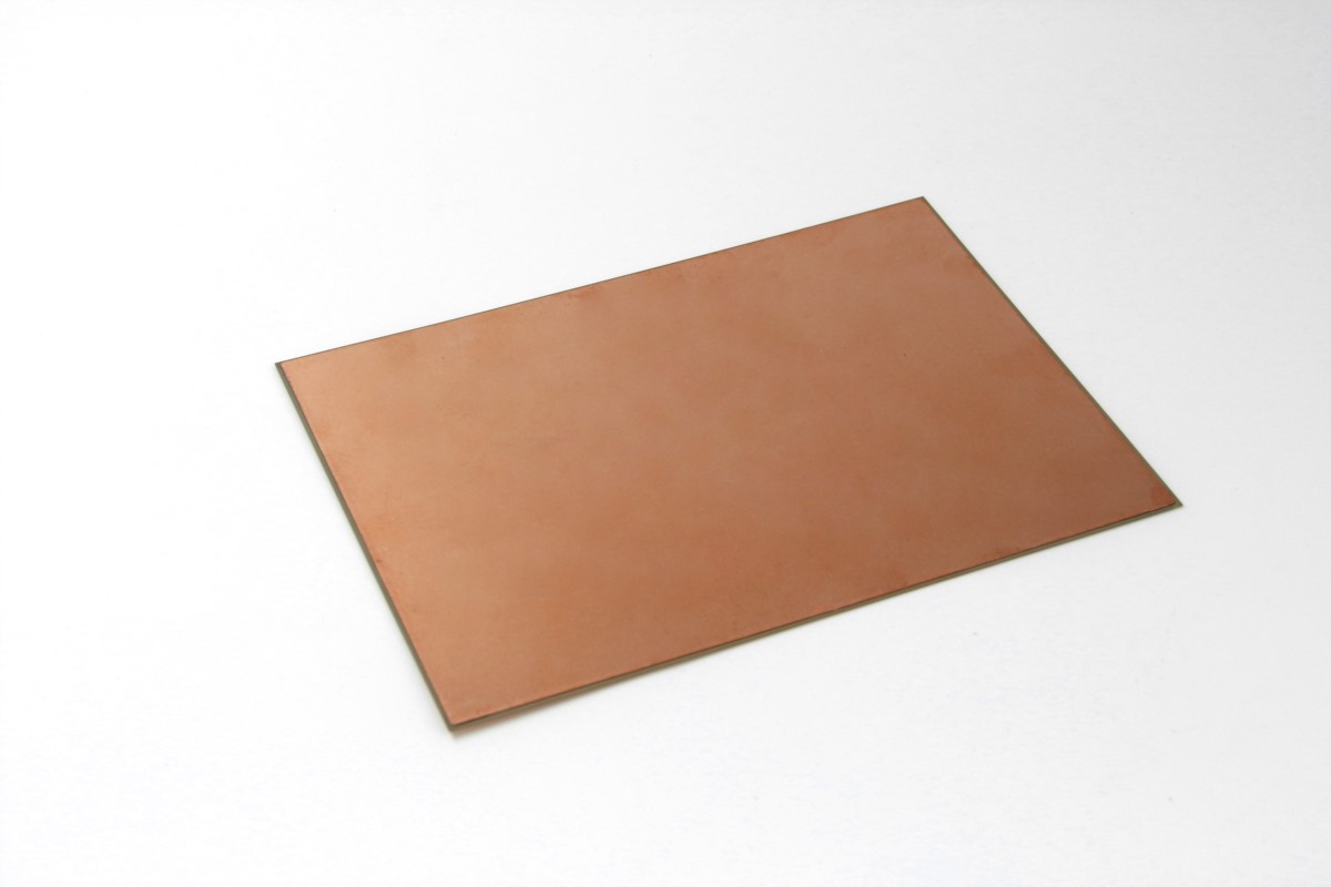
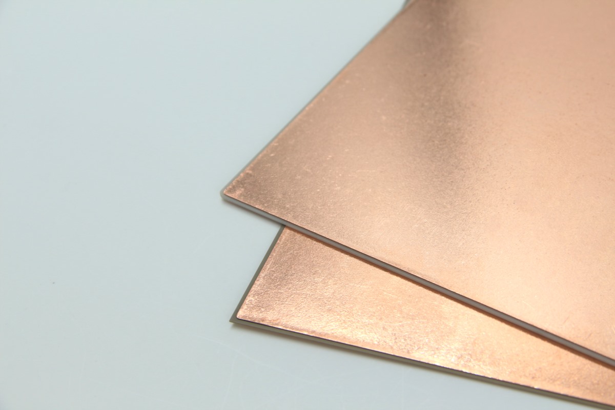
– Could have different thickness of copper on one plate;
– Environmental frindly;
– Strong cold and heat resistance;
– Easy full automation, production efficiency high, low production cost;
– Copper thickness 0.1-0.5mm,very suitable for high power device packaging.
Applications:
– SiC power modules
– IGBT modules
– Electric drive inverters
– Photovoltaic inverters
– Wind energy converters
– Industrial frequency converters
– High-power switching power supplies
– 5G base station power supplies
– High-power power supplies for data centers
– Communication RF modules
Properties
| Material | Item | Value |
| Si3N4 | Composition | 96% SiN |
| Thickness (mm) | 0.2,0.32,0.35,0.635,0.4-1.5 | |
| Density(g/cm3) | 3.2±0.25 | |
| Thermal Conductivity (20℃,W/m·k) | 85+ | |
| Flexural Strength (MPa) | 700-800 | |
| Dielectric Constant (IMHz) | 8 | |
| Dielectric Loss (IMHz) | 0.001 | |
| Dielectric Strength (KV/mm) | 20 | |
| Volume Resistivity (Ω/cm) | 1014 | |
| ALN | Composition | 96% ALN |
| Thickness (mm) | 0.25,0.32,0.635 | |
| Density (g/cm3) | 3.3 | |
| Thermal Conductivity (20°C,W/m·k) | 170+ | |
| Flexural Strength (MPA) | 350 | |
| Dielectric Constant (IMHz) | 9 | |
| Dielectric Loss (IMHz) | 0.0005 | |
| Dielectric Strength (KV/mm) | 20 | |
| Volume Resistivity (Ω/cm) | 1014 | |
| Copper | Material | Oxygen-free Copper |
| Purity (%) | 99.99 | |
| Hardness (HV) | 60-110 | |
| Conductivity (MS/m) | 58.6 | |
| Thickness (mm) | 1.2,1.0,0.8,0.5,0.4,0.3,0.25,0.2 | |
| AMB Substrate |
Largest Size (mm) | 190*140 |
| Line Spacing (mm) | ≥0.5 | |
| Line Width (mm) | Customized | |
| Peel Strength of Copper Layer (minimum) (N/mm) |
>10 | |
| Solderability(%) | >95% | |
| Delivery Method | Small Pieces or Panel | |
| Surface States (um) | CU/AU/AG |
Declaration: This is an original article of INNOVACERA®. Please indicate the source link when reprinting: https://www.innovacera.com/product/amb-ceramic-substrate.
 Enquiry