.svg)
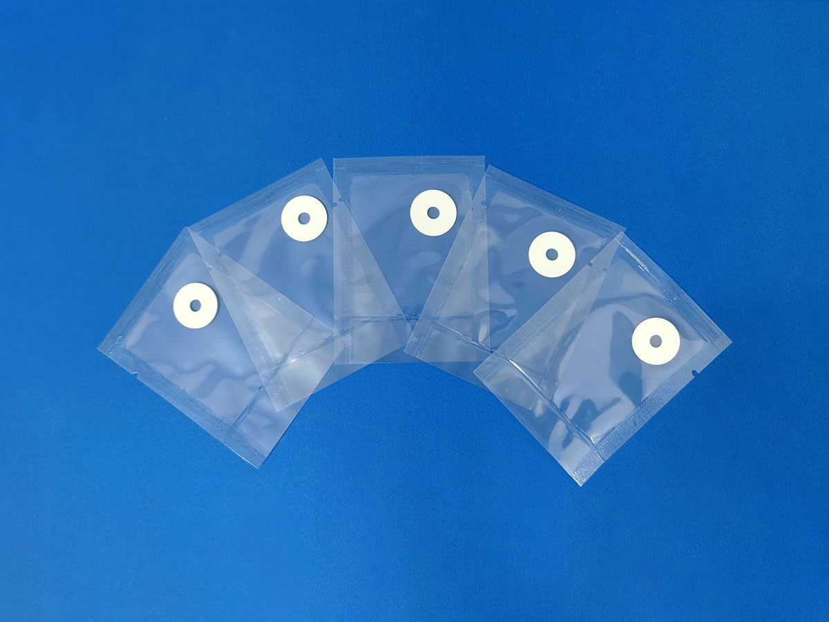
Pyrolytic Boron Nitride is also called PBN. It also has a hexagonal crystal structure like hot-pressed boron nitride ceramic but is produced in different manufacturing processes. PBN is produced by chemical vapor deposition (CVD), no need to go through the traditional hot pressing sintering process. The purity is up to 99.99%. Benefiting from the high purity, good thermal stability, and chemical inertness, PBN ceramic is suitable for semiconductor components or vacuum systems. It is widely used to produce ceramic crucibles for single crystal growth of compound semiconductors (such as GaAs, InP, etc.), crucibles for molecular beam epitaxy, crucibles for OLED, etc.
Main properties of PBN ceramic
- Good thermal conductivity
- High insulation resistance
- High dielectric strength over wide temperature ranges.
- Extremely pure
- Non-wetting
- Non-toxic
- Non-reactive to most other compounds
- Withstands high temperatures and rapid cooling
Declaration: This is an original article of INNOVACERA®. Please indicate the source link when reprinting: https://www.innovacera.com/news/high-purity-pbn-washer.html.


 Enquiry