.svg)
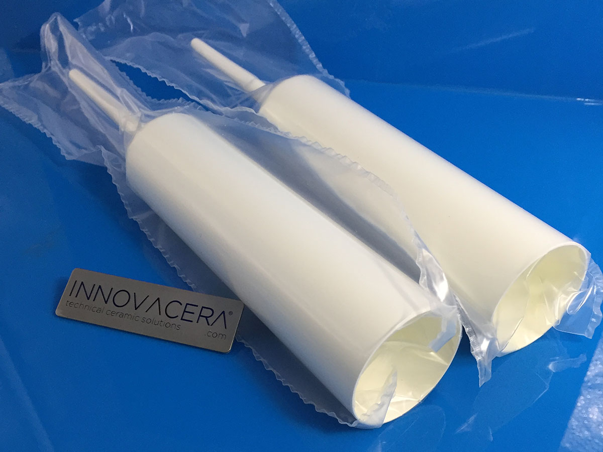
The key material for the growth of indium phosphide (InP) is single crystal-pyrolytic boron nitride (PBN)
Since 2002, scientists have jointly developed a new type of semiconductor material that can enable communication satellites to transmit data at extremely high speeds in space. This new material is called indium phosphide (InP).
InP is an important compound semiconductor material and is a new generation of microelectronics and optoelectronic functional materials following silicon (Si) and gallium arsenide (GaAs). Indium phosphide semiconductor materials have the advantages of high electronic limit drift speed, good radiation resistance, and good thermal conductivity. Compared with gallium arsenide semiconductor materials, it has the characteristics of high breakdown electric field, thermal conductivity, and average electron velocity.
InP single crystal growth methods mainly include high-pressure liquid-sealed Czochralski (LEC) and vertical gradient solidification (VGF). The key container for these two single crystal growth methods is the PBN crucible. Pyrolytic Boron Nitride (PBN) is a special ceramic material, which is produced by INNOVACERA company by chemical vapor deposition on special equipment. PBN crucible has the advantages of high purity, high-temperature resistance, acid, alkali, salt, and organic reagents, high temperature and most molten metals, semiconductors, and other materials non-wetting, non-reaction, etc., is the best container for indium phosphide single crystal growth.
InP semiconductor materials have a wide bandgap structure, and the speed of electrons passing through the indium phosphide material is fast, which means that devices made of this material can amplify signals of higher frequency or shorter wavelength. Therefore, satellite signal receivers and amplifiers made of indium phosphide chips can work at extremely high frequencies above 100 GHz, have a wide bandwidth, are less affected by the outside world, and have high stability. Therefore, indium phosphide is a more advanced semiconductor material than gallium arsenide, which may promote the development of the satellite communications industry to higher frequency bands.
Declaration: This is an original article of INNOVACERA®. Please indicate the source link when reprinting: https://www.innovacera.com/news/single-crystal-pyrolytic-boron-nitride.html.


 Enquiry