.svg)
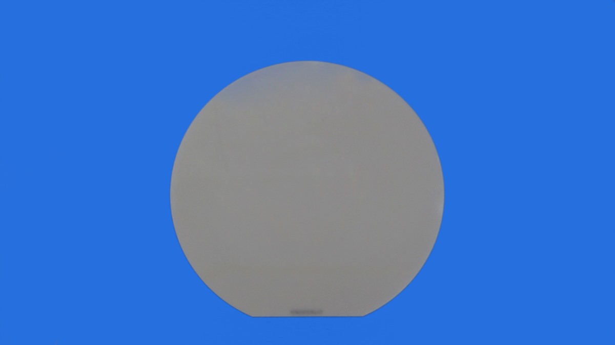
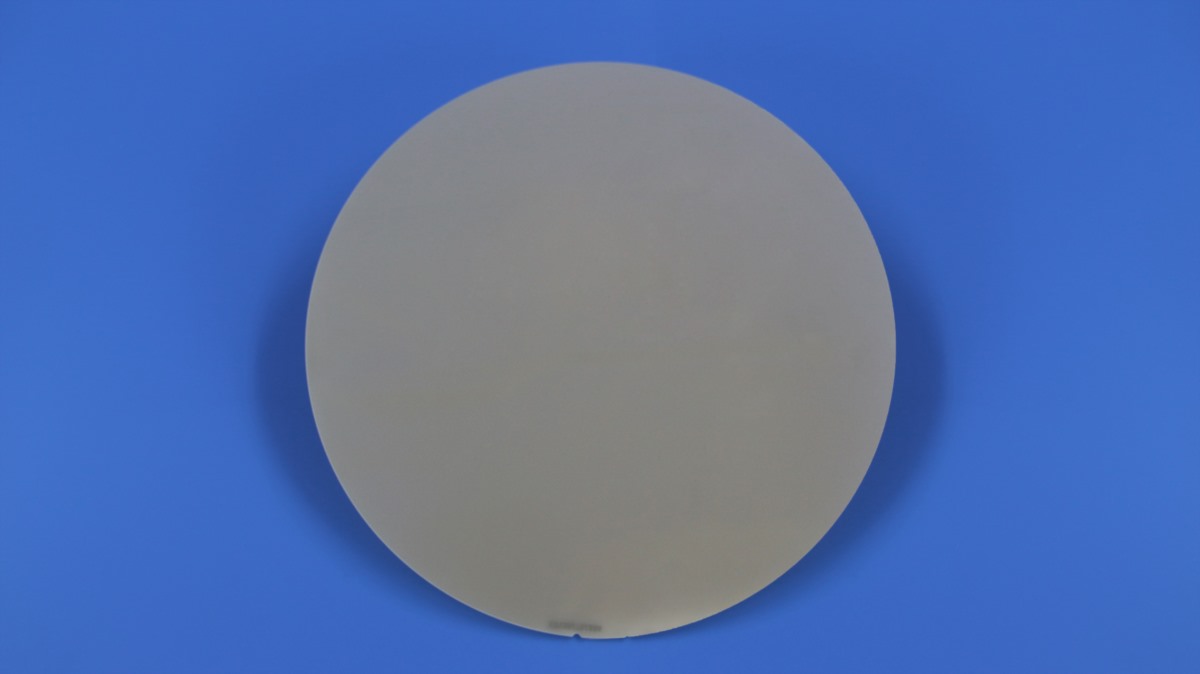
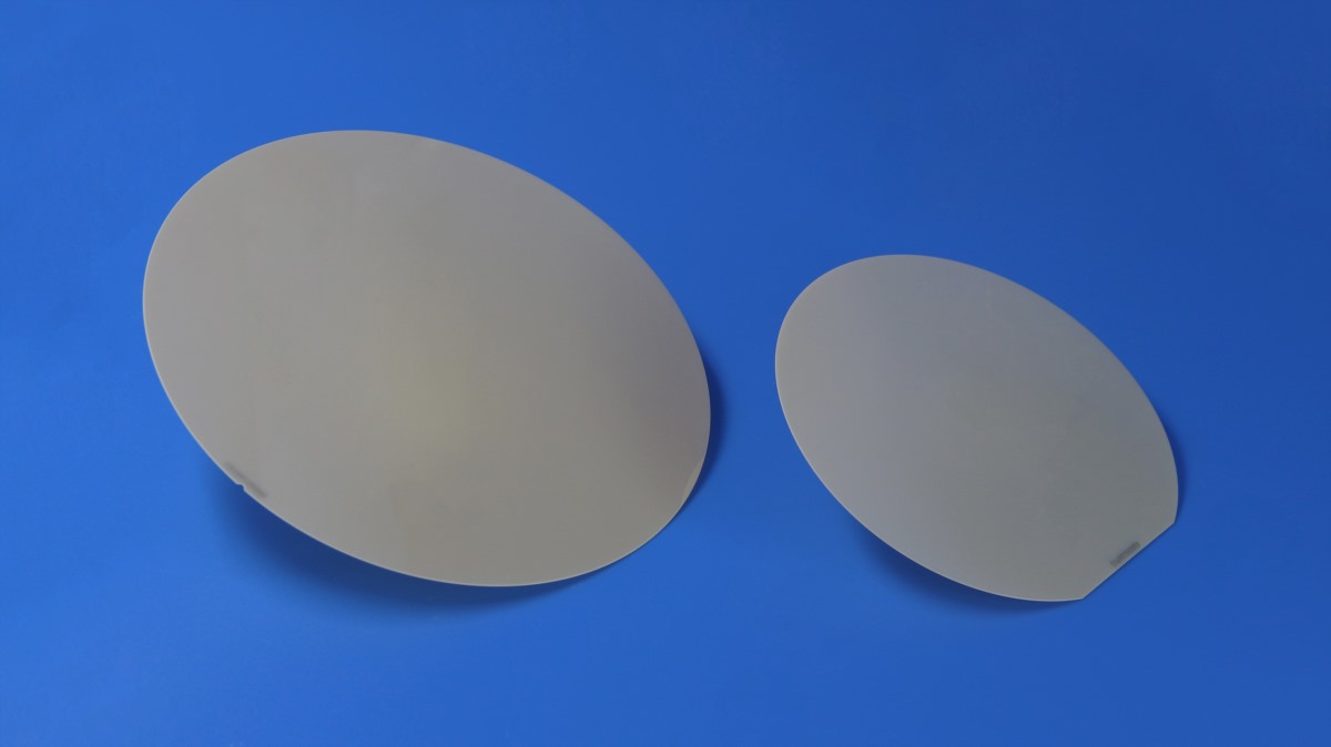
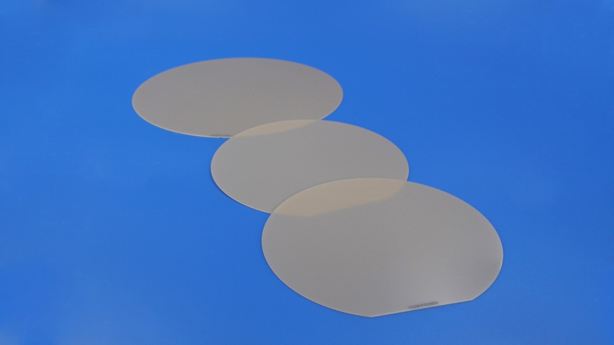
Aluminum Nitride (AIN) materials play a important roles in the semiconductor industry, the similarities between its thermal profile and that of silicon has made an ideal choice for wafer-related semiconductor applications. Innovacera’s Aluminum nitride wafers have high reliability of Si chip and thermal heat cycling.
According to direct wafer bonding technology, polished semiconductor wafers can be bonded together without adhesives. Direct wafer bonding requires very flat and high smooth surface (Ra≤0.05um), Innovacera AlN wafers substrate can meet this requirements.
Features
- High melting point
- High electrical insulation
- Lowdielectric constant
- Higher mechanical strength
- Superior corrosion resistance against molten metal
- Thermal and chemicalstability
- High thermal conductivity (170-220w/mk)
- Similar coefficient of thermal expansion to that of silicon (si)
Properties
| Properties | Unit | AN170 | AN230 | AN99 | AN999 |
| Color | – | Gray | Beige | Gray | Beige |
| Content of ALN | – | ≥95% | ≥96% | ≥99% | ≥99.9% |
| Bulk Density | g/cm3 | ≥3.30 | ≥3.28 | ≥3.26 | ≥3.25 |
| Flexural Strength | MPa | ≥400 | ≥300 | ≥300 | ≥300 |
| Compressive Strength | MPa | 2500 | 2000 | 2000 | 2000 |
| Hv 500g | Gpa | 10.5 | 9.0 | 9.0 | 9.0 |
| Young’s Modulus | Gpa | 300 | 300 | 280 | 280 |
| Thermal Conductivity (@20°C) | W/m·K | ≥170 | ≥220 | ~100 | ~90 |
| Specific Heat | KJ/(Kg·K) | 0.74 | 0.73 | 0.73 | 0.73 |
| C.T.E (r.t.-400°C) | 10-6/K | 4.6 | 4.6 | 4.6 | 4.6 |
| Volume Resistivity | Ω·cm 20°C | ≥1014 | ≥1013 | ≥1010 | ≥1010 |
| Dielectric Strength | KV/mm | ≥16 | ≥15 | ≥15 | ≥15 |
| Dielectric Constant (@1MHz) | – | 8.6 | 8.6 | 8.6 | 8.6 |
| Loss Tangent (@1MHz) | ×10-4 | 5 | 5 | 5 | 5 |
AlN Wafers Specification
| Properties | Unit | 6″ Wafer | 8″ Wafer |
| Material | – | AlN Ceramics | AlN Ceramics |
| Thermal Conductivity | W/m·K | >170 | >170 |
| Thermal Expansion Coefficient | ppm/K(300~1200K) | 4-6 | 4-6 |
| Sintering Aid | – | Y2O3 | Y2O3 |
| Diameter | mm | 150+/-0.25 | 200+/-0.25 |
| Notch Depth | mm | 1.0+0.25/-0/Locating Edge | 1.0+0.25/-0 |
| Notch Angle | – | 90°+5/-2° | 90°+5/-2° |
| Thickness | μm | 400±15 | 400±15 |
| TTV | μm | <10 | <10 |
| BOW | μm | <±30 | <±30 |
| Warp | μm | <50 | <50 |
| Ra | nm | <50 | <50 |
Applications
- Semiconductor manufacturing
- Microwave power amplifier
- Rf powerand switch
- High temperature power electronics
- Laser diode dispersionoptoelectronic devices
- High power and high frequency electronic devices
- MOSFET, IGBTpower modules
- Led packages for cooling and protecting circuits
Declaration: This is an original article of INNOVACERA®. Please indicate the source link when reprinting: https://www.innovacera.com/product/aluminum-nitride-wafer-substrates.
 Enquiry