.svg)
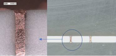
The Through Ceramic Via (TCV) interconnection technology is an innovative approach for high-density three-dimensional packaging. Traditional ceramic substrate metallization schemes often encounter challenges such as residual liquid inside the holes, poor adhesion, and incomplete copper filling. TCV technology, however, employs a copper paste filling method for ceramic vias, offering a simple process, complete filling, strong adhesion, and low cost.
Innovacera utilizes a sintered copper paste composed of micro-nano composites, ensuring excellent electrical conductivity and reliability. By incorporating high-temperature binders and special fillers, it’s possible to further adjust the thermal expansion coefficients of the copper via and interface, thereby achieving high-reliability copper via connections.
The TCV process flow chart

Process Characteristics:
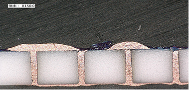
– Wide range of depth-to-diameter ratios, with excellent flowability of the paste resulting in complete adhesion to the hole walls.
– Dry process, eliminating the residue of chemicals from copper plating.
– High process efficiency, as all holes can be completely filled by printing alone.
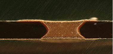
– High reliability, with adjustable thermal expansion coefficients.
– High efficiency, high quality, and low cost of vacuum filling process.
– Achieving effective conduction of high current with electrical resistivity close to pure copper.
– High reliability achieved through hole copper with low thermal expansion coefficient and interface layer.
Process Advantages:
1. Small dielectric constant, excellent high-frequency characteristics, reducing signal delay time.
2. Thermal expansion coefficient closer to silicon, as inorganic substrate materials generally have lower coefficients than organic ones.
3. Strong heat resistance, with inorganic substrate materials having higher glass transition temperatures than organic ones, making them less prone to damage during thermal shock and cycling.
4. High thermal conductivity, enabling efficient dissipation of heat generated by high-density packaging.
5. High mechanical strength and good dimensional stability, ensuring high component installation precision.
6. Strong chemical stability, resistant to corrosion from acids, alkalis, and organic solvents during processing, without experiencing discoloration, swelling, or other characteristic changes.
7. Excellent insulation performance, ensuring high reliability.
Processing Capabilities:
| Substrate | Aluminum Oxide | Aluminum Nitride |
| Thermal Expansion Coefficient | 6.8 ppm/K | 4.7 ppm/K |
| Thermal Conductivity | 23 W/m·K | 170 W/m·K |
| Dimensions | <182 x 182 mm | <120 x 120 mm |
| Thickness | 0.25 – 1 mm | 0.15 – 0.63 mm |
| Hole Diameter | >60 μm | >60 μm |
| Depth-to-Diameter Ratio | <10:1 | <10:1 |
| Hole Spacing | >0.1 mm | >0.1 mm |
Application:
– High-power electrical power electronic modules, solar panel components for high-frequency switching power supplies, solid-state relays.
– Automotive electronics, lasers, CMOS image sensors.
– High-power LED lighting products.
– Communication antennas, automotive ignition systems.
If you’re interested in the aforementioned materials technology, feel free to reach out to us at +86-592 5589730 or via email at sales@innovacera.com for further discussion and communication. We look forward to hearing from you!
Declaration: This is an original article of INNOVACERA®. Please indicate the source link when reprinting: https://www.innovacera.com/news/an-introduction-to-through-ceramic-via-tcv-interconnection-technology.html.


 Enquiry