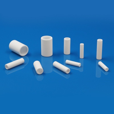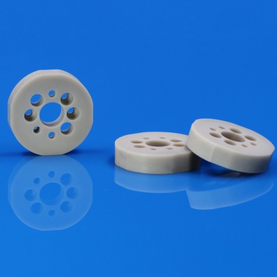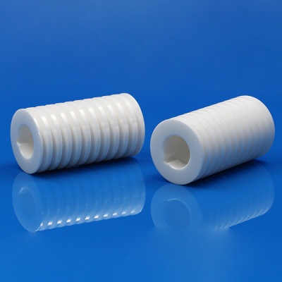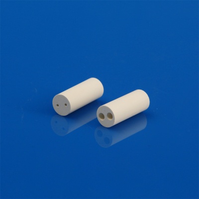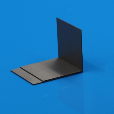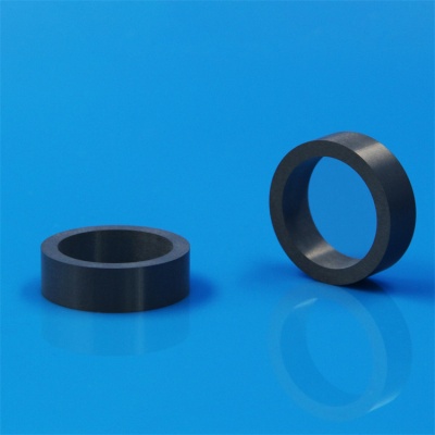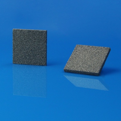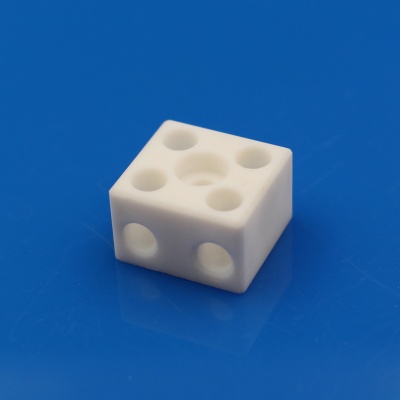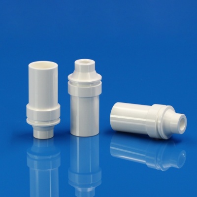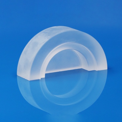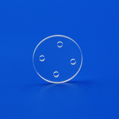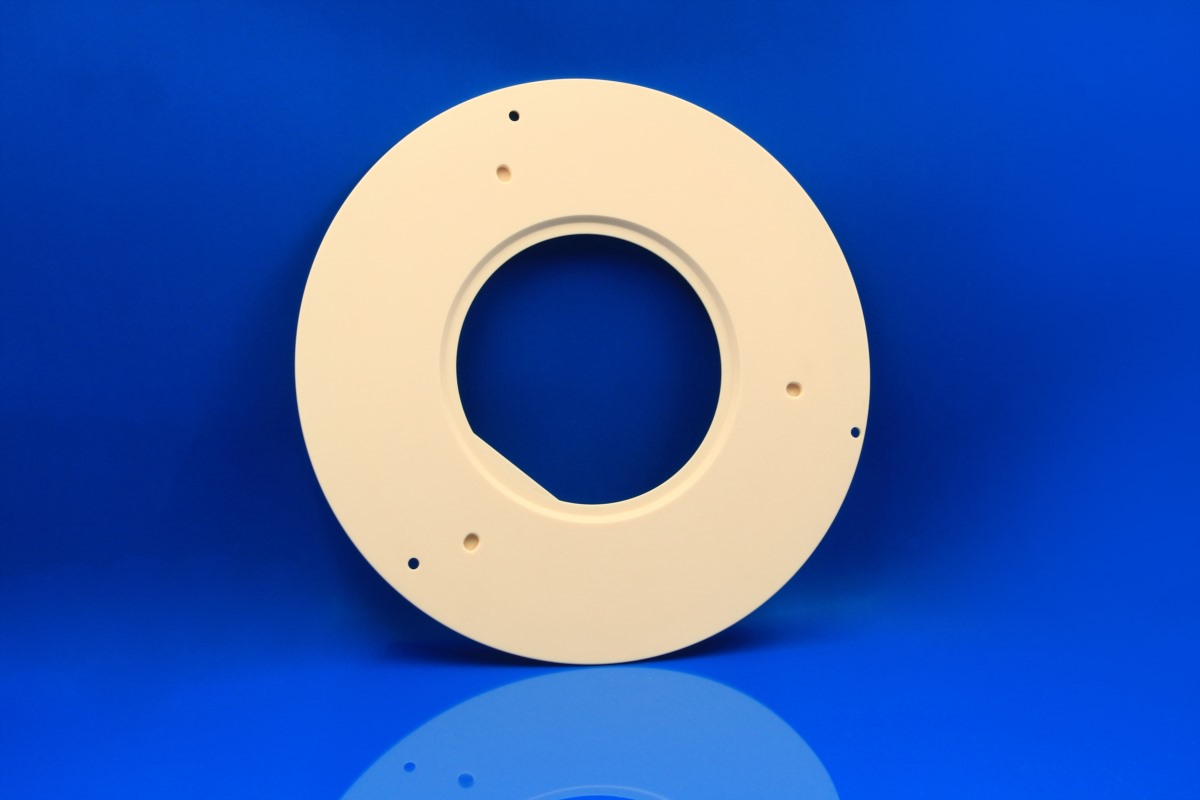


Alumina Ceramic Focus Rings serve as critical components within plasma etch equipment, primarily in the etch chamber. The rings are strategically positioned to optimize plasma distribution and maintain uniformity during the etching process.
Semiconductor manufacturing processes demand operation within cleanroom environments, especially for components utilized under high-temperature, vacuum, and corrosive gas conditions. Ceramic materials maintain high stability within these complex physical and chemical environments.
The Ceramic Focus Ring is a critical part for the Semiconductor Etch Process. When aluminum alloy is chosen as the etch chamber material, it can easily cause metal particle contamination. Therefore, high-purity (over 99.5%) alumina ceramic is used in the manufacturing of Ceramic Focus Rings as the chamber material for plasma etching equipment.
Ceramic Focus Rings characteristics:
-Wear Resistance,
-Corrosion Resistance,
-Excellent Mechanical Properties,
-Electrical Insulation,
-Meet the quality standard of semiconductor product.
Innovacera have rich experiences in technical ceramic solution, advanced ceramic component and semiconductor industry more than 10 years. We have established a high standard of quality system and strict quality control process, each batch of products are subjected to strict quality inspection. The service philosophy of Innovacera is meeting quality requirement and customer satisfaction.
If you need the alumina Ceramic Focus rings, welcome to contact us.
Declaration: This is an original article of INNOVACERA®. Please indicate the source link when reprinting: https://www.innovacera.com/product/alumina-ceramic-focus-rings
Frequently Asked Questions
Why Are High-Purity Alumina Focus Rings Vital in Plasma Etching? How Do They Improve Wafer Edge Uniformity?
In semiconductor etch chambers, metallic parts trigger destructive metal-particle contamination and create non-uniform plasma sheath boundaries at the wafer perimeter. INNOVACERA’s >99.5% high-purity alumina ceramic focus rings maintain stable electrical insulation and plasma distribution right up to the wafer bevel edge. Designed to pair seamlessly with electrostatic chucks (e-chucks), they resist corrosive halogen process gases, reduce micro-arcing defects, and dramatically improve edge-die process yield in high-vacuum environments.
Need Plasma-Resistant Chamber Parts for Semiconductor Tools? How to Order Custom Ceramic Focus Rings from INNOVACERA?
Semiconductor wafer manufacturing requires extreme dimensional tolerances and cleanroom-grade surface finishes. INNOVACERA provides custom alumina ceramic focus rings machined to sub-millimeter precision for 200 mm and 300 mm etching systems. Customers can send their equipment chamber drawings, gas operating conditions, and purity specifications (over 99.5% Al2O3) to receive high-precision parts with full CMM inspection validation.