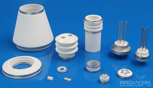
Ceramic materials, which have excellent properties such as high hardness, high abrasion resistance and high corrosion resistance, but with poor electrical conductivity and weldability to limit their application. While metallization is a process of coating metal on the surface of ceramics, which can improve the conductivity and weldability of ceramics, thus expanding their range of applications. Ceramic after metallization has high thermal conductivity, insulation, heat resistance, strength and coefficient of thermal expansion that matched with the chip, and gradually developed into the ideal packaging substrate for new generation of integrated circuits, as well as power electronic modules.
The common ceramic substrate materials can be metallized include Al2O3, SiC, AlN and Si3N4.
1. Thick Film Metallization
Thick film metallization is a metal paste coated on the ceramic surface through the screen-printing method, and then after high temperature drying and heat treatment to form a metalized ceramic substrate technology. The advantage of this technology is that the process is simple and cost-effective cost, while the disadvantage is that the electrical performance of the conductive line is poor, can only be used for lower power and size requirements of the electronic devices.
2. Direct Bonded Copper
DBC (Direct Bonded Copper, DBC) is a copper foil (thickness greater than 0.1 mm) directly bonding to the surface of the Al2O3 ceramic substrate, in the N2 protection and temperature range of 1065 ℃ -1083 ℃. Pure copper in the molten state do not need to wet Al2O3, it needs to bring in oxygen elements in the reaction process, Cu-Cu2O eutectic liquid generated at high temperature has a good wettability on Al2O3, through the generation of CuAlO2 as a transition layer, you can be directly laying the copper foil on the Al2O3 ceramic substrate.
3. Thin Film Metallization
Thin film metallization is carried out in high vacuum conditions, with physical methods of solid material surface ionization for ions, followed by low-pressure gas in the ceramic substrate surface deposition of the required film process, that is, the physical vapor deposition technology ( PVD ), mainly including magnetron sputtering coating, deposition of a thin layer of Cu layer as a seed layer in the ceramic surface, so that the subsequent plating process to carry out. Electroplate is then performed to thicken (protect) the seed Cu. Then through the film, exposure, development and other processes to complete the transfer of graphics, and then plating so that the Cu layer grows to the required thickness, and finally through the film, etching process to complete the production of conductive lines.
Such ceramic substrate using thin-film process has shown great competitiveness in power LED packaging in recent years.
In summary, ceramic metallization can ensure the ceramic materials own the electrical and thermal conductivity of metal, thus expanding their applications including electronics, automotive sensors, optical devices, medical devices, and aerospace etc.
Declaration: This is an original article of INNOVACERA®. Please indicate the source link when reprinting: https://www.innovacera.com/news/know-more-about-ceramic-metallization-when-ceramic-perfectly-bond-with-metal.html.


 Enquiry