In high-temperature experiments and material processing, the crucible is not merely a container for loading materials; it directly affects the purity of the materials, the stability of the process, and the performance of the final product.
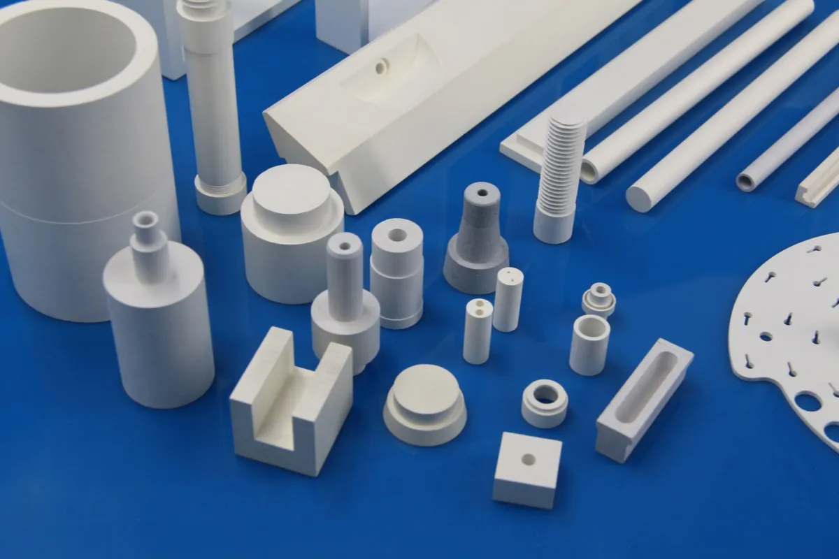
For common crucible materials such as alumina, zirconia, and silicon nitride, they can already meet the needs of most industrial scenarios. However, in some cases where the requirements are extremely high and the working conditions are more demanding, boron nitride crucibles often become the indispensable alternative.
So in what scenarios must we prioritize the use of boron nitride crucibles?

I.. When the melt fails to adhere: Non-wetting properties determine process quality
1. Principle Analysis
Boron nitride has an extremely low surface energy and exhibits excellent non-wetting properties towards various molten substances, meaning that the molten material is not likely to spread or adhere to its surface.
In contrast:
· Alumina: Can be partially wetted by certain metals
· Zirconia: Exhibits adhesion phenomena in specific systems
This means that the BN crucible can achieve a more “clean” release of the material.
2. Application Case: Aluminum Liquid Treatment
During the melting process of aluminum and aluminum alloys, common problems include:
· The molten metal adheres to the inner wall of the crucible
· The pouring is not thorough
· Residues affect the purity of the next batch
After using boron nitride crucibles:
· The molten aluminum hardly adheres
· It can be completely poured out
· The frequency of cleaning is significantly reduced
Applicable scenarios: Metallurgical processing of non-ferrous metals, glass treatment, salt melt process technology
II. When purity is of utmost importance: Chemical inertness prevents contamination
1. Principle Analysis
Boron nitride exhibits extremely strong chemical stability:
· It does not react with the melt
· It does not release impurity elements
· It does not introduce ion contamination
In contrast, some oxide ceramics may undergo interface reactions or element migration at high temperatures.
2. Application Case: Processing of High-Purity Metals (Ga / In)
In the semiconductor field, materials such as gallium (Ga) and indium (In) are extremely sensitive to purity:
· Even a small amount of contamination can affect electrical performance
· The requirements for container materials are extremely high
After using boron nitride crucibles:
· Effectively prevent impurities from being introduced
· Maintain the high purity of the material
· Meet the requirements of semiconductor-level processes
Applicable scenarios: Semiconductor material preparation, single crystal growth, functional material development

III. When there is a significant temperature variation: The thermal shock resistance is more reliable.
1. Principle Analysis
Boron nitride possesses:
· Low thermal expansion coefficient
· Excellent thermal shock resistance
· Good structural stability
Can withstand the stress changes caused by rapid heating and cooling.
2. Application Case: Laboratory Rapid Thermal Cycling
In scientific research experiments, crucibles often require:
· Multiple rapid heating and cooling cycles
· Local heating (such as induction heating)
· Frequent repeated use
After using boron nitride crucibles:
· Significantly reduce the risk of cracking
· Extend service life
· Improve experimental efficiency
Applicable scenarios: Material testing, research and development experiments, heat treatment processes
IV. When in a Vacuum or Inert Atmosphere: Significant Advantages in Environmental Stability
1. Principle Analysis
Boron nitride exhibits excellent stability in the following environments:
· Vacuum
· Inert atmospheres such as nitrogen and argon
· Reductive atmosphere
However, it should be noted that:
Boron nitride begins to oxidize in the air at approximately 800–900℃. It is not suitable for long-term high-temperature oxidation environments and is more suitable for use in a vacuum or inert atmosphere.
2. Application Case: Vacuum Evaporation and PVD Process
During the vacuum evaporation process, the crucible needs to withstand high temperatures for a long time and remain clean.
After using boron nitride crucibles:
· No contamination of the evaporation materials
· The process becomes more stable
· Extends the service life of the equipment
Applicable scenarios: Vacuum coating, powder sintering, high-temperature experimental equipment
V. Comparison of Properties of Different Crucible Materials
| Performance Dimension |
Boron Nitride (BN) |
Alumina (Al₂O₃) |
Zirconia (ZrO₂) |
Silicon Nitride (Si₃N₄) |
| Non-wettability |
⭐⭐⭐⭐⭐ |
⭐⭐ |
⭐⭐⭐ |
⭐⭐⭐ |
| Chemical Stability |
⭐⭐⭐⭐⭐ |
⭐⭐⭐ |
⭐⭐⭐ |
⭐⭐⭐ |
| Thermal Shock Resistance |
⭐⭐⭐⭐⭐ |
⭐⭐ |
⭐⭐⭐ |
⭐⭐⭐⭐ |
| Operating Atmosphere |
Vacuum / Inert |
Air |
Air / Controlled |
Inert |
| Cost |
Relatively High |
Low |
Medium |
Relatively High |
VI. How to Select the Appropriate Crucible Material?
In practical applications, material selection should be based on the core requirements of the process:
· If cost and versatility are the priorities: alumina can be given priority consideration.
· If high-temperature structural stability is the concern: zirconia or silicon nitride can be chosen.
· If high purity, non-wetting or thermal shock resistance are required: boron nitride has more advantages.
VII. Conclusion
The selection of crucible material essentially matches the process requirements.
When your application involves the following key conditions:
· The melt does not adhere
· High purity control
· Intense temperature changes
· Vacuum or inert atmosphere
Boron nitride crucibles are often not only a better choice, but even the only feasible solution.
For different sizes, structures and application requirements, boron nitride crucibles also support customized designs to meet diverse industrial and scientific application scenarios. Please contact sales@innovacera.com for more information.


 Enquiry