technical ceramic solutions

News

Category Archives: News

Ceramic Precision Ball Selection Guide: G Grades, Performance and Applications

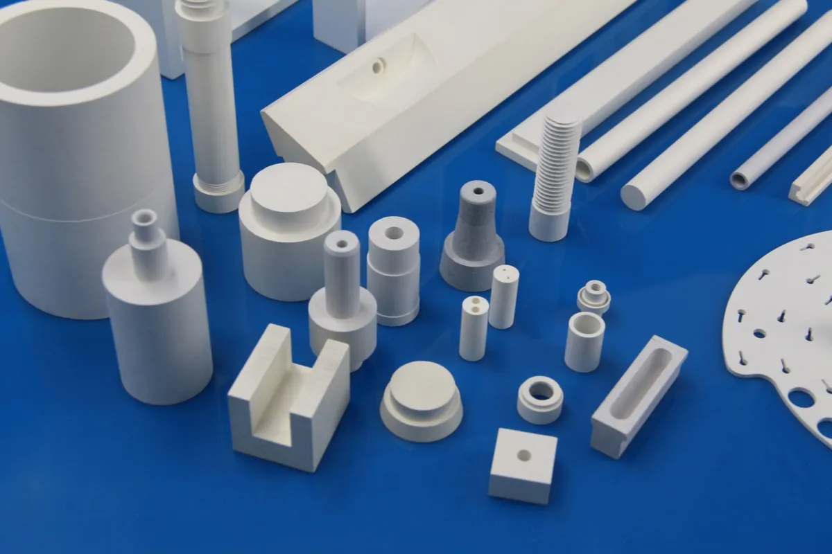
In the field of high-end equipment manufacturing, precision spheres are one of the key fundamental components that affect the performance and stability of the equipment. Compared with traditional steel balls, ceramic precision balls, due to their superior physical and chemical properties, are being widely applied in demanding working conditions, such as precision bearings, fluid control systems, and semiconductor equipment, etc.


During the actual selection process, in addition to the material’s own properties, the geometric accuracy of the sphere is also of great significance. During the actual selection process, in addition to the material’s own properties, the geometric accuracy of the sphere is also of great significance. Among them, the common G10, G5, G3, etc. G grades are important indicators for evaluating the precision level of ceramic precision balls.


I. What is a ceramic precision ball?


The ceramic precision balls are high-precision spherical components made of high-performance ceramic materials (such as zirconia, silicon nitride, and alumina) through precise molding, sintering, and multiple grinding and polishing processes.


Compared with traditional steel balls, its core advantages include:


  • Low density: Lighter in weight, which helps reduce centrifugal force and energy consumption.
  • High hardness and wear resistance: Significantly extend service life
  • Excellent corrosion resistance: Suitable for acidic, alkaline and complex medium environments
  • Excellent thermal stability: suitable for high-temperature or temperature-varying environments
  • Electrical insulation and non-magnetic properties: Suitable for electronic, medical and semiconductor equipment

Thanks to these characteristics, ceramic precision balls perform exceptionally well in high-speed, high-temperature, highly corrosive and highly clean environments.


Zirconia ceramic precision balls


II. G Grade: The Precision Measurement Standard for Ceramic Precision Balls


In practical applications, ceramic balls not only need to have “good material quality”, but also must be “precisely manufactured”.


The G grade is precisely an important indicator for measuring its geometric accuracy. The G grade is usually based on international standards such as ISO 3290 and ANSI/ABMA, and is mainly used to describe the following aspects:


  • Ball diameter variation (consistency of diameters in the same batch)
  • Spherical error (roundness)
  • Surface quality (control of microscopic defects)
  • Batch stability


Basic rule: The smaller the G-level value is, the higher the accuracy will be, and the stricter the requirements for manufacturing and testing capabilities will be.


It should be noted that there may be differences in the specific value definitions among different standard systems and manufacturers. The actual selection should be confirmed in accordance with the technical specifications.


III. Common G-levels and Their Application Scopes

G Grade Precision Level Key Characteristics (Engineering View) Typical Applications Technical Reference (Typical Range)
G200–G50 General Industrial Grade Larger dimensional tolerance, for low-speed or non‑precision applications Agricultural machinery, standard bearings, basic mechanical structures Diameter tolerance: ≥5 μm
G25–G10 Standard Industrial Grade Balanced cost & performance, suitable for most industrial uses General bearings, pump & valve systems, home appliances Diameter tolerance: approx. 0.25–1 μm
G5 Medium‑High Precision Excellent dimensional consistency, stable operation, low vibration Automotive bearings, high‑speed motors, precision equipment Diameter tolerance: approx. 0.1–0.5 μm
G3 High Precision Minimal geometric error, for high‑speed & high‑stability applications High‑speed spindles, precision instruments, semiconductor equipment (partial) Sub‑micron level control
G1–G0 Ultra‑High Precision Near‑perfect spherical form, extremely high machining & inspection requirements Aerospace, high‑end instruments, advanced manufacturing systems Ultra‑low tolerance (near nano‑level control)


IV. How to Select the Appropriate G Level?


In practical engineering applications, the selection of the G grade requires comprehensive consideration of the following three core factors:


1.Equipment performance requirements


For high-speed, high-precision or high-load equipment, it is recommended to use higher-grade ceramic balls to enhance operational stability and reduce vibration and wear.


2.Operating environmental conditions


In environments with high temperatures, corrosive conditions or high cleanliness requirements, ceramic materials should be given priority, and a higher G grade should be combined to ensure reliability.


3. Cost and Performance Balance


As the grade increases to G level, the processing difficulty and testing requirements significantly rise, and the cost also increases accordingly. Therefore, under the premise of meeting the performance requirements, an appropriate grade should be selected to achieve the best cost-performance ratio.


V. The application value of ceramic precision balls compared to steel balls


Under the same precision level, ceramic precision balls usually offer better overall performance:


  • Lower friction and wear
  • More stable high-speed operation capability
  • Longer service life
  • Better environmental adaptability


Silicon nitride ceramic precision balls


Therefore, in high-end manufacturing and in harsh working conditions, ceramic balls are gradually replacing traditional steel balls and have become one of the key basic components.


VI. Conclusion


Currently, Innovacera can consistently supply ceramic precision ball products ranging from G3 to G200, covering various material systems such as zirconia, silicon nitride, and aluminum oxide. It supports multiple size specifications and can meet the usage requirements ranging from general industrial applications to medium to high precision scenarios.


If you need product parameters, selection suggestions or customization plans, please feel free to contact sales@innovacera.com.


Boron nitride ceramic nozzles: The revolutionary in high-temperature processes and lead the high-temperature spraying revolution

Boron nitride ceramic nozzles are widely used in high-temperature spraying, grinding, and jetting due to their excellent wear resistance, high temperature resistance and corrosion resistance. They can provide efficient, precise and stable nozzle performance.


Application cases of boron nitride ceramic nozzles:


1. Powder metallurgy nozzles: Boron nitride ceramic nozzles play an important role in powder metallurgy processes. Due to their excellent wear resistance and high temperature resistance, they can be used for high-temperature jetting of particles, powders, and coating materials. Boron nitride ceramic nozzles can provide a stable jet flow to ensure a precise and uniform powder metallurgy process.


2. Large-size amorphous ribbon nozzles: Boron nitride ceramic nozzles are key components in the planar flow casting process for preparing amorphous alloy ribbons, requiring stable operation under extreme conditions (high temperature, high-speed melt erosion, rapid solidification). The main performance requirements for these nozzles are: excellent resistance to thermal shock and thermal expansion coefficients, resistance to metal corrosion, good wear resistance and low hardness, and minimal difference in thermal conductivity between the pressure direction and the horizontal direction. High consistency in amorphous alloy products is also crucial. Boron nitride perfectly meets these requirements, making it the most suitable material.


3. Abrasive nozzles: Boron nitride ceramic nozzles are widely used in the field of abrasive jetting. Due to their excellent wear resistance and corrosion resistance, they can provide long-term stable jetting effects in high-speed, high-pressure and high-concentration abrasive flows. Boron nitride ceramic nozzles can be used in abrasive jetting equipment, surface treatment and cleaning, etc., effectively improving the efficiency and quality of abrasive jetting.


4. Burner nozzles: Boron nitride ceramic nozzles play an important role in the field of burners. Due to its excellent high temperature resistance and wear resistance, it can be used for the injection and regulation of high temperature burners. Boron nitride ceramic nozzles can provide stable combustion injection, improve combustion efficiency and stability, and reduce energy waste and pollutant emissions.


5. Air atomization nozzles: Boron nitride ceramic nozzles are widely used in the fields of coating, spraying and atomization. Due to its stable injection performance and corrosion resistance, it can be used for the injection of high temperature spraying liquids, powders, and aerosols. Boron nitride ceramic nozzles can provide uniform spraying and atomization effects and realize precise and efficient coating and spraying processes.


boron nitride nozzles, the revolutionary in high-temperature processes


In short, Boron nitride ceramic nozzles have excellent wear resistance, high temperature resistance and corrosion resistance, and play an important role in powder metallurgy, amorphous ribbon manufacturing, abrasive blasting, burners, and coating spraying.


Different types of boron nitride are used in scenarios with different usage environment requirements. Below is the datasheet.


Properties Units BMA BSC BMZ BSN
Main Composition BN+ZR+AL BN+SIC BN+ZRO2 BN+SI3N4
Color White Graphite Greyish-Green White Graphite Dark Gray
Density g/cm3 2.25-2.35 2.4-2.5 2.8-2.9 2.2-2.3
Three-Point Bending Strength MPa 65 80 90 150
Compressive Strength MPa 145 175 220 380
Thermal Conductivity W/m·k 35 45 30 40
Thermal Expansion Coefficient (20-1000℃) 10-6/K 2 2.80 3.5 2.80
Max Using TemperatureIn AtmosphereIn Inactive GasIn High Vacuum (Long Time) (℃) 90017501750 90018001800 90018001800 90018001800
Room Temperature Electric Resistivity Ω·cm >1013 >1012 >1012 >1013
Typical Application Powder Metallurgy Powder Metallurgy Metal Casting Powder Metallurgy
High Temperature Electrical Furnace Components
Metal Vaporize Crucible
The Container of Metal or Glass Melting
The Casting Mould Components of The Precious Metal and Special Alloy.
High Temperature Support Part
Nozzle and Transport Tube of The Melting Metal
Nitrides Sintering(Sagger and Setter Plate)


For more information, Welcome to contact sales@innovacera.com.


Semicon Southeast Asia 2026 Exhibition and High-Performance Materials Trends

Participate in the Semicon Southeast Asia 2026 in Kuala Lumpur to explore the application trends of boron nitride, micro porous ceramics and alumina substrates, aluminum nitride substrates in power devices, electronic packaging and precision processing, and seize the innovation opportunities in the Asia-Pacific semiconductor industry.


About the Semicon Southeast Asia 2026


In 2026, Semicon Southeast Asia 2026 will witness its annual grand event – the Semiconductor Exhibition at the Kuala Lumpur International Convention Centre.This exhibition brings together the world’s leading suppliers to showcase the latest applications and technical cases of boron nitride, micro porous ceramics, alumina substrates, aluminum nitride substrates and precision machined parts.Next, we will comprehensively introduce the exhibition bright spot, key material trends and application cases, helping enterprises and engineers understand the latest developments of advanced semiconductor materials in the fields of power devices, electronic packaging and precision processing.Semicon Southeast Asia 2026 bright spot and information


  • Time and Place: May 5-7, 2026, Kuala Lumpur International Convention Centre
  • Exhibition participating companies and products: Covering local and international suppliers, with a focus on showcasing high-performance substrates, precision ceramic parts and power heat dissipation components and so on


Item Details
Year / Edition 2026 / 31st Edition
Format In-Person
Gross Area > 24,000 sqm
Targeted Companies > 500 International & Local Companies
Number of Booths > 1,000 Booths
Expected Attendees 15,000 – 20,000
Show Hours 9:00 – 17:00
Expected Audiences’ Profile Industry Leaders, Government Agencies, SMEs, Media


Boron nitride plate for the semiconductor industry

Aluminum nitride wafers for semiconductors


Main material trends and application


Boron Nitride Advantages and Semiconductor Application


  • High thermal conductivity and excellent electrical insulation
  • Heat dissipation for power devices and intelligent packaging
  • Exhibition cases: LED heat sinks, microelectronic packaging

Porous Ceramics For Microelectronic Packages


  • High-temperature stability and lightweightHigh-density electronic packagingExhibition example: Heat dissipation structure of semiconductor modules

Alumina and Aluminium Nitride Substrates


Alumina: Moderate cost, suitable for conventional power devicesAluminum nitride: High thermal conductivity, dimensional stabilityExhibition Cases: Power Modules and Precision Packaging

Alumina and aluminum nitride substrates were displayed on Semicon Southeast Asia 2026


Precision Machining Ceramic Components


    • Processing of complex micro-structures
    • Semiconductor packaging, optoelectronic devices
    • Application illustration of aluminum nitride substrate and precision ceramic parts
    • The heat dissipation module of the power device adopts microporous ceramics and boron nitride.


aluminum nitride precision machined ceramic parts used in the heat dissipation module of the power device

Alumina precision machined parts displaying at the Kuala Lumpur Semiconductor Exhibition


The advantages of Malaysia’s semiconductor industry


  • Asia-pacific semiconductor manufacturing base, Kuala Lumpur and Penang industrial parks
  • Complete supply chain and policy support
  • Display the practical application and demand of materials in the local industry

Contact us for further discussion


Our boron nitride, micro porous ceramics, alumina and aluminum nitride substrates , precision machined parts have been widely applied in Asia, Europe and the United States. Application fields: Heat dissipation of power devices, microelectronic packaging, and processing of complex and fine structures.The materials displayed at this exhibition are only some of the cases. For enterprises that need high-performance heat dissipation, precise packaging and customized substrates, we welcome you to contact us for more professional advice or visit our booth L2 2591 for further discussion.


Application of alumina machining parts at the Kuala Lumpur Semiconductor Exhibition

Aluminum nitride and wafer applications at the Kuala Lumpur Semiconductor Exhibition


High-Precision Alumina Ceramic Packaging Enclosures: Unlocking High-Reliability Packaging for High-End Electronic Devices

In the era of rapid evolution toward high-density integration, high-power output, and miniaturized design in electronic technology, packaging enclosures serve as the “protective core” and “performance carrier” of electronic devices. The quality of such packaging components exerts a decisive influence on the operational stability, service life, and application adaptability of the corresponding electronic devices. It can be regarded as one of the key indicators that dominate the overall performance and service reliability of the devices. Especially in core strategic fields including integrated circuits, optical communications, microwave devices, and automotive electronics, the performance requirements for packaging enclosures are becoming increasingly rigorous and demanding. Specific indicators such as hermeticity, electrical insulation, thermal dissipation efficiency, electromagnetic anti-interference capability, and dimensional processing accuracy are all subject to higher technical standards. High-precision alumina ceramic packaging enclosures, relying on their outstanding inherent material properties, mature and controllable manufacturing processes, as well as diversified and complete product series, have gradually emerged as the optimal selection to satisfy the advanced packaging requirements of high-end electronic devices. These advantages enable them to provide stable and reliable packaging support for cutting-edge electronic components, thereby continuously injecting impetus into the high-quality and sustainable development of the electronic information industry.


1. Core Material Properties: Multiple Advantages Drive Packaging Upgrades


High-precision alumina ceramic packaging enclosures adopt high-purity alumina ceramic as their core substrate material. During the preparation process, such substrates are produced through strict and precise ingredient proportioning as well as specialized high-temperature sintering procedures. These advanced preparation methods help to form a highly dense and uniformly distributed internal microstructure. As a result, the final product integrates a variety of superior comprehensive properties covering electrical, mechanical, and thermal performance aspects.


Superior Electrical Insulation: The mass fraction of alumina in the ceramic substrate is controlled within the range of 92% to 93%. At a standard room temperature of 20℃, the volume resistivity of the material can reach as high as 10¹⁴ Ω·cm. Even when exposed to a high-temperature environment of 300℃, it still maintains a stable insulation level of 10¹⁰ Ω·cm. When the temperature rises to 500℃, the volume resistivity remains at 10⁸ to 10⁹ Ω·cm. Such excellent and stable insulation performance can effectively isolate external electromagnetic interference. It can also prevent internal short-circuit risks of the circuit system. This provides reliable and long-lasting electrical protection for core functional components such as integrated circuit chips. Therefore, this material is especially suitable for the packaging requirements of high-frequency and high-voltage electronic devices.


Excellent Mechanical Strength: The flexural strength of the alumina ceramic substrate can be stably maintained at 400 MPa. It presents outstanding resistance to mechanical impact and periodic vibration loads. This enables the packaging structure to effectively withstand various external forces encountered during device transportation, assembly, and actual service. It can significantly reduce the probability of structural deformation or fracture damage. At the same time, the material itself has extremely high hardness and excellent wear resistance. These characteristics help maintain the structural integrity of the packaging shell over a long service period. They also effectively extend the overall service life of the entire electronic device.


Efficient Heat Dissipation and Thermal Stability: The thermal conductivity of the ceramic substrate can reach 18 to 20 W/(m·K). Such thermal conductivity enables rapid and effective conduction and dissipation of the heat generated by the chip during continuous operation. It can effectively avoid performance degradation or service life reduction caused by local overheating inside the device. The thermal expansion coefficient of the material is precisely regulated and controlled. Within the temperature range of 40℃ to 400℃, its thermal expansion coefficient is 6.7 to 7×10⁻⁶/℃. Within the temperature range of 400℃ to 800℃, the thermal expansion coefficient is 6.9 to 7.2×10⁻⁶/℃. This value is highly matched with the thermal expansion characteristics of chips, metal leads, and other connected components. Such high matching degree can effectively reduce the thermal stress concentration generated during repeated high and low temperature cycles. It also greatly lowers the risk of cracking or interface separation failure of the packaging structure.


Stable Dielectric Performance: Under the test frequency of 1 MHz, the dielectric constant of the material is maintained between 9 and 10. The dielectric loss tangent value is only 4×10⁻⁴. Such excellent dielectric properties can effectively reduce the energy loss and signal attenuation during high-speed signal transmission. They can fully ensure the communication quality and strict signal integrity of high-frequency devices. Therefore, this material can well adapt to high-speed signal transmission scenarios including microwave communication, optical communication, and other related fields.


2. Precision Manufacturing Process: Full-Process Quality and Accuracy Control


The excellent performance of alumina ceramic packaging enclosures stems from precise manufacturing and strict quality control throughout the entire process. The production process covers multiple core processes, each achieving high-precision control.


Core Production Processes: From tape casting, blanking, drilling, hole filling, and screen printing, to cavity opening, lamination, pressing, cutting, sintering, and then to metallization, nickel plating, mounting and brazing, and gold plating, a complete independent production chain is formed. All processes are closely linked, ensuring the stability of product structure and performance through professional equipment and technical experience.


Dimensional Accuracy Control: The external dimensions range from 2mm to 100mm. The tolerance of common dimensions (5mm~75mm) is precisely controlled to ±1%, and the tolerance of specially customized dimensions can be controlled within ±0.6%. In terms of thickness, conventional products are 0.8mm~4.0mm with a tolerance of ±3%, while special thin products can be as thin as 0.4mm with a tolerance of only ±2%. The minimum single-layer thickness is 0.1mm with a tolerance of ±0.01mm.


Internal Structure Processing Accuracy: The minimum hole diameter can reach 0.08mm with a tolerance of ±0.01mm, and the tolerance of conventional hole diameters (0.13mm~0.42mm) is also maintained at ±0.01mm. The hole spacing and the distance from the hole to the edge strictly follow the minimum standard of 3 times the hole diameter to ensure structural stability. The via position deviation does not exceed ±0.015mm to ensure accurate circuit connection.


Metallization Process Standards: The minimum line width can reach 0.05mm with a tolerance of ±10%, and the minimum line spacing is 0.05mm with a tolerance of ±0.01mm. The metal layer is treated with nickel plating, gold plating, and other processes, featuring uniform thickness, excellent conductivity, and oxidation resistance, meeting the welding and long-term use needs of devices.


3. Diverse Product Series: Precise Adaptation to Multi-Scenario Needs


Alumina ceramic packaging enclosures form a complete product series covering different application scenarios, including five core types. Each series of products is optimized for specific needs, adapting to the packaging of diverse electronic devices.


Ceramic Small Outline Package (CSOP): Adopts a miniaturized structure and wing-shaped leads, with small stress and strong resistance to mechanical impact. It supports multiple lead pitches such as 1.27mm, 1.00mm, and 0.80mm, with the number of leads ranging from 4 to 56. The cavity size and external dimensions can be flexibly customized, widely used in the packaging of various high-reliability integrated circuits and precision components, especially suitable for scenarios requiring both volume and stability.


Ceramic Small Outline Package (CSOP)


Ceramic Surface Mount Power Package (SMD): Features strong conductive current capacity, with a large-area heat sink in the chip bonding area and excellent heat dissipation performance. The number of leads is 2~3, and the cavity size ranges from 2.60mm×2.60mm to 10.00mm×9.60mm. It is an ideal packaging choice for microwave devices, crystal oscillators, and crystal oscillation devices, adapting to the heat dissipation and performance needs of high-power devices.


Ceramic Surface Mount Power Package (SMD)


Ceramic Dual In-Line Package (CDIP): Adopts a dual in-line lead design, with the number of leads ranging from 4 to 40 and pitches covering 0.8mm, 2.54mm, and other specifications. The sealing forms include flat sealing and gold-tin sealing. It is suitable for the packaging of various integrated circuits, optocouplers, MEMS, and other products with low requirements on the number of leads and assembly density, featuring convenient installation and strong compatibility.


Ceramic Leadless Chip Carrier/Quad Flat No-Lead Package (CLCC/CQFN): Boasts small parasitic parameters and compact volume, supporting both double-sided and four-sided lead-out structures. The lead pitches include 1.27mm, 1.00mm, 0.50mm, etc., with the number of leads ranging from 4 to 48. It adapts to the high-density surface mounting needs of VLSI, ASIC, ECL, and other circuits, widely used in high-integration circuit devices.


Ceramic Leadless Chip Carrier/Quad Flat No-Lead Package (CLCC/CQFN)


Optical Communication Device Package (ROSA/TOSA): Specifically designed for the optical communication field, it features high airtightness and reliability, and can meet the requirements of multiple application rates from 10GHz to 400GHz. It is suitable for various optoelectronic transmitting devices, receiving devices, optical switch modules, and high-power lasers, providing core guarantee for the stable transmission of optical communications.


Optical Communication Device Package (ROSA/TOSA)


4. Wide Application Fields: Empowering the High-Quality Development of the Electronic Industry


With multiple advantages, alumina ceramic packaging enclosures have been deeply integrated into various core industrial fields, becoming an indispensable key component of high-end electronic devices.


In the field of industrial control, such high-performance packaging components are well suited for the assembly and protection of various integrated circuits and precision functional components, as they can maintain highly stable working performance under complex and harsh industrial application environments, while their outstanding anti-interference capacity can effectively ensure the long-term continuous and stable operation of key industrial equipment; in the field of automotive electronics, these packaging products possess excellent resistance to repeated high and low temperature shocks and severe mechanical vibration loads, enabling them to maintain structural integrity and functional stability under severe vehicle-mounted working conditions, and accordingly, they can provide safe, stable, and highly reliable packaging protection for vehicle-mounted chips, high-precision sensors, and other core electronic components. In the optical communication field, ROSA/TOSA packages support high-speed transmission, helping to upgrade optical communication technology. In fields such as microwave devices and crystal oscillators, the efficient heat dissipation and conductive performance of SMD series products ensure the stable output of device performance.


With the continuous popularization of technologies such as 5G, artificial intelligence, and the Internet of Things, electronic devices will have increasingly higher requirements for the performance of packaging enclosures. Alumina ceramic packaging enclosures will further break through the performance boundaries of miniaturization, high heat dissipation, and high airtightness through material formula optimization, process upgrading, and structural innovation, providing stronger support for the innovative development of the electronic information industry, helping more high-end electronic devices achieve performance upgrading and scenario expansion. Contact sales@innovacera.com for more information.


Ceramic Slitting Blade Solutions for High-Speed Slitting of LLDPE Films Process—Industrial Application Case

This case study carried out optimization practices on the issues of tool life and powder control during the slitting process of high-toughness polyethylene film, increasing the service life of the blade from approximately 3 days to about 7 days.


I. Project Background


In the field of film slitting processing, the performance of the cutting tools directly affects the cutting quality, production efficiency, and the operational stability of the equipment. One of our film processing customers mainly produces linear low-density polyethylene (LLDPE) films and metallocene linear low-density polyethylene (mLLDPE) films. Compared with ordinary LLDPE materials, mLLDPE has higher toughness and tensile strength, and it requires higher wear resistance and sharpness retention of the cutting tools during high-speed slicing.


The customer’s production line operates at 500 m/min, a typical high-speed cutting condition. This poses continuous challenges to the stability and lifespan of the cutting tools.


II. Core Pain Points of Customers


Previously, the customer had been using tungsten steel (metal) blades for a long time. In actual production, they mainly encountered the following problems:


  • Shorter lifespan: After continuous use for approximately 3 days, obvious cutting powder will appear, and the tool wears out more rapidly. Frequent shutdowns for replacement are required.
  • Friction and contamination issues: During the high-speed slicing process of LLDPE / mLLDPE films, the friction coefficient is relatively high, which can lead to the generation of powder and affect the cleanliness of the products.
  • Insufficient adaptability of high-toughness materials: In the cutting process of mLLDPE films, the cutting edges are more prone to dulling and the stability decreases.
  • Production efficiency is limited: Frequent tool changes result in a decline in production line continuity, increasing maintenance and downtime costs.


III. Solution: Zirconia ceramic slotting slicing blade


According to the customer’s working conditions, we recommend replacing it with a zirconia ceramic slot-cutting blade.


Zirconia ceramic slotting slicing blade


Compared with traditional tungsten steel cutting tools, ceramic blades have the following advantages:


  • High hardness and excellent wear resistance: It can maintain a sharp state for a long time during high-speed cutting, effectively delaying the wear of the cutting edge.
  • Low friction characteristics: The cutting process is smoother, effectively reducing heat generation due to friction and the phenomenon of material dragging.
  • Excellent anti-adhesion property: Reduces the adhesion of debris from high-molecular materials such as polyethylene, thereby reducing the generation of powder at the source.
  • Structural stability: Under stable installation and high-speed operation conditions, it can meet the requirements of continuous cutting operations.


The objective of this application is clear: Extend the service life of the blade, reduce cutting powder, and enhance the stability of high-speed cutting.


IV. Application Results


After continuous on-site testing by the customer and actual production verification, the ceramic blades have shown stable performance and achieved significant improvements:


– Significantly extended service life

After continuous use for approximately 7 days, slight powdering begins to occur with the ceramic blade. Compared to the original tungsten steel blade (which lasts about 3 days), the service life is approximately doubled, effectively reducing the frequency of changing blades and the downtime.

– The powder issue has been significantly improved

The powder generation cycle during the cutting process has been significantly prolonged, while the product cleanliness and production stability have been improved, resulting in reduced subsequent cleaning and maintenance costs.

– Stable operation under high-speed conditions

Under the high-speed cutting condition of 500 m/min, the blade operates stably as a whole and can meet the requirements of a continuous production rhythm.


V. Optimization Direction


During the actual application process, the customers reported that when cutting the slightly wrinkled film, there was some fluctuation in the uniformity of the local surface.


This phenomenon is mainly related to the following factors:


The blade remains sharp with periodic changes.

Film tension control status

Sensitivity of material flatness under high-speed conditions


Currently, the customers are adjusting the production process parameters further to optimize the blade usage cycle and operating conditions, to enhance the overall cutting consistency and stability.


Ceramic Slotted Blades


VI. Summary and Application Value


This case has verified the excellent compatibility of ceramic slicing blades in the high-speed slicing of high-toughness films such as LLDPE and mLLDPE:


Through this application, the customer achieved:


The service life has been increased from approximately 3 days to approximately 7 days, representing a nearly 2-fold improvement.

The generation of fragmented powder was significantly delayed, and the cleanliness of the product was noticeably improved.

Maintain stable operation capability under a 500 m/min high-speed condition.


This solution effectively helped the customer achieve cost reduction, efficiency improvement, and enhanced production stability, providing a more reliable tool selection for the processing of high-toughness films.


Innovacera offers a variety of advanced ceramic cutting tools and customized solutions, which are widely used in film cutting, packaging processing, electronic materials, and high-end industrial manufacturing. If you are interested, please contact sales@innovacera.com.


Why Ceramic Substrates Fail: Cracking, Warpage and Metallization Problems Explained

Ceramic substrates are widely used in power electronics, LED packaging, and semiconductor applications due to their excellent electrical insulation, high thermal conductivity, and chemical stability. However, during the actual manufacturing and service process, ceramic substrates may still encounter various reliability failure issues, among which the more typical ones include: cracking, warping, and metallization structure failure.

In most cases, these failures are not caused by a single factor, but by the combined effects of material properties, structural design, and manufacturing processes.


I. Cracking of Ceramic Substrate: A typical brittle fracture failure


1. Typical Failure Modes

The cracking of ceramic substrates typically manifests as:

Cracks occur during processing or assembly

Breakage occurs during reflow soldering or brazing

Cracks propagate during thermal cycling tests and lead to failure


2. Root Causes


(1) Thermal stress mismatch

There is a significant difference in thermal expansion coefficients between ceramic materials (such as Al2O3, AlN) and metals (such as Cu, Au). During the temperature cycling process, interface thermal stress is generated, which is an important driving force for crack initiation and propagation.


(2) Surface/subsurface defects introduced during processing

During the processes of cutting, slicing, grinding or drilling, microcracks or residual damage layers may be introduced. These defects may expand into through-cracks under the subsequent thermal mechanical loading.


(3) Structural stress concentration

Sharp corner structures, insufficient clearance around holes, or local section changes can all lead to local stress concentration, thereby reducing the reliability of the structure.


3. Recommended Solutions

Optimize the structural design to avoid sharp corners and high-stress concentration areas

Improve the processing quality to reduce micro-cracks and processing damage layers

Prioritize the use of material systems with higher fracture toughness in high-reliability applications (such as using AlN to replace part of Al2O3 in certain applications)


Aluminum Nitride Substrate


II. Ceramic substrate warping: Overall deformation caused by thermal-mechanical mismatch


1. Typical Failure Modes

Warpage typically appears as overall bending or distortion of the substrate after sintering or subsequent processing.

The flatness is insufficient during SMT assembly.

Structural deformation after reflow soldering leads to uneven welding stress.


2. Main Mechanism


(1) Thermal stress imbalance caused by asymmetric structure

In DBC/AMB or metallized ceramic structures, single-sided or asymmetric metal layers can lead to uneven thermal expansion constraints, thereby causing warping.


(2) Temperature gradient during sintering process and difference in shrinkage

During the sintering process, if there is an uneven temperature field or if the temperature rise and drop rate control is improper, it may lead to differences in the densification behavior in different areas, thereby generating residual stress.


(3) Differences in material density and tissue uniformity

Uneven density distribution of the preform or differences in local porosity can lead to inconsistent sintering shrinkage, thereby causing macroscopic deformation.


(4) The thickness and distribution of the metal layer have an impact (particularly significant for DBC/AMB)

In the DBC structure, the thickness and distribution of the copper layer have a significant impact on the warpage behavior, and are often one of the dominant factors.


3. Recommended Solutions

Optimize the structural design and adopt symmetrical metallization structures as much as possible.

Control the sintering curve, reduce the temperature gradient and the accumulation of thermal stress.

Improve the uniformity of the ceramic body density.

In the DBC/AMB design, reasonably match the copper thickness and the distribution of the patterns.


Metallized Ceramic Substrate


III. Metallization Failure: The result of the combined effect of interface and fatigue.


1. Typical Failure Modess

Local peeling or overall delamination of the metal layer

Failure of the pad or interruption of the conductive path

Decrease in electrical connection reliability after thermal cycling


2. Main mechanism


(1) Interfacial bonding degradation

In the DBC (Direct Bonded Copper) or AMB (Active Metal Brazing) systems, the bonding between ceramics and metals relies on the interface reaction layer or transition layer structure. If the interface reaction is insufficient or fails, it will result in a decrease in bonding strength.


(2) Thermal cycle fatigue accumulation

Due to the difference in thermal expansion coefficients between ceramics and metals, under the long-term action of thermal cycling loads, the interface shear stress accumulates continuously, eventually leading to fatigue damage and delamination.


(3) Process-related defects

Including but not limited to:

Poor control of copper layer oxidation (key factor in DBC process)

Insufficient wetting of active metals (key factor in AMB process)

Pores (voids) or unbound areas

Uneven local interface reactions


3. Recommended Solutions


Optimize the process parameters of DBC/AMB to enhance the uniformity of interface reactions

Strictly control the oxygen content and the atmosphere environment (especially during the copper oxidation process of DBC)

Improve the wetting and diffusion quality of the active layer in AMB

Carry out systematic thermal cycling reliability verification (Thermal Cycling Test)


IV. Systematic Influencing Factors Affecting the Reliability of Ceramic Substrates


In practical engineering applications, the reliability of ceramic substrates is usually determined by the following three levels together:


1. Material level

Aluminum oxide (Al₂O₃): Mature and stable, with lower cost

Aluminum nitride (AlN): High thermal conductivity, suitable for high power density scenarios

Silicon nitride (Si₃N₄): High strength and high reliability, suitable for demanding working conditions


Silicon Nitride Substrate


2. Structural Design Aspects

Stress Concentration Control (Holes, Boundaries, Corners)

Distribution of Copper Layers and Symmetry Design

Optimization of Thermal-Mechanical Load Paths


3. Manufacturing Process Aspects

Temperature uniformity control during sintering process

Quality control of metallization interface

Control of processing damage and optimization of post-processing techniques


V. Conclusion


The failure of ceramic substrates is not usually caused by a single factor, but rather is the result of the combined effects of material performance limitations, the rationality of the structural design, and the control level of the manufacturing process.

In high-reliability applications (such as IGBT power modules, SiC devices, and high-power LED packaging), it is necessary to comprehensively optimize the material selection, structural design, and process control from a system perspective in order to reduce the failure risk caused by thermal-mechanical coupling stresses.


Innovacera can offer ceramic substrates covering materials such as alumina, aluminum nitride, and silicon nitride, as well as metallization solutions like DBC, AMB, and DPC. It also supports customized design and application selection optimization. For technical support, material selection, or custom designs, feel free to contact us at sales@innovacrea.com or send your drawings for evaluation.


How to Choose The Most Suitable High-Temperature Ceramic Components To Improve Furnace Efficiency & Extend Service Life

From semiconductor chips to new energy vehicles, and from steel metallurgy to environmental protection, high-temperature ceramic components support the development of high-end manufacturing with their unique performance advantages.


In modern industrial systems, furnace systems are the core equipment for material synthesis, heat treatment, energy conversion, and environmental protection. Whether it’s the diffusion process of semiconductor wafers, the sintering of lithium battery cathode materials, the continuous casting of steel, or the regenerative combustion of industrial waste gases, these processes are inseparable from extreme conditions such as high temperature, corrosion, wear, and thermal shock.


Their characteristics—high melting point, high hardness, chemical inertness, thermal shock resistance, and electrical insulation—make them key to overcoming these “metal bottlenecks.”


Ultra High Temperature Ceramics Insulator Tubes for Furnaces


INNOVACERA provides the following ceramic components for various furnace systems.


1. Boron Nitride Ceramics (BN)

Furnace System Type Application Area Key Components Specific Application Method
Vacuum Furnaces, Crystal Growth Furnaces Compound Semiconductors, Vacuum Coating Crucibles, Evaporation Boats, Insulators Crystal growth for wafer materials, or evaporation for OLEDs, metal coatings.
Powder Metallurgy Sintering Furnaces Powder Metallurgy, Cemented Carbides Sintering Boats, Mold Release Coatings Holds metal powders during sintering, preventing adhesion to the boat.
Hot Pressing, Pressureless Sintering, Gas Pressure Sintering Furnaces Electronic Ceramic Substrates, Power Semiconductors Setter Plates, Hot Pressing Molds, Multi-layer Ceramic Clamps Carries ceramic substrates (e.g., AlN, Si₃N₄) during sintering at 1600°C–1900°C without sticking or contamination.
High-Temperature, High-Pressure Equipment Composite Materials Hot Pressing Molds, Seals Densification and forming of carbon/carbon composites and ceramic matrix composites.


2. Alumina Ceramics (Al₂O₃)

Furnace System Type Application Area Key Components Specific Application Method
Tube Furnaces, Box Furnaces Semiconductor/Photovoltaic, Lab Research Furnace Tubes, Chambers Serves as a sample container for high-temperature sintering, diffusion, and annealing in controlled atmospheres.
Pusher Furnaces, Shuttle Kilns Lithium Battery Cathode Materials, Electronic Ceramics Saggars, Pusher Plates Used in continuous production for sintering materials like LFP, NMC, and electronic ceramic components.
Single Crystal Growth Furnaces Semiconductors, Optical Crystals Crucibles, Insulation Layers Provides a stable, pure thermal environment for growing crystals like sapphire and silicon.


3. Silicon Carbide Ceramics (SiC)

Furnace System Type Application Area Key Components Specific Application Method
Roller Hearth Kilns, Tunnel Kilns Building Ceramics, Lithium Battery Materials Kiln Rollers, Roller Bars Transports ceramic tiles at 1200°C–1300°C or carries saggars during lithium cathode sintering.
Circulating Fluidized Bed Boilers Power Generation, Solid Waste Treatment Air Nozzles, Separator Liners Resists erosion and corrosion from high-speed coal powder or waste fuel, extending equipment life.
High-Temperature Heat Exchangers Petrochemicals, Waste Heat Recovery Honeycomb Regenerators, Heat Exchange Tubes Utilizes high thermal conductivity for efficient heat exchange, resistant to high-temperature corrosive gases.
Waste Incinerators Solid/Hazardous Waste Treatment Thermocouple Protection Tubes, Grate Bars Protects sensors from erosion by high-temperature corrosive flue gases.


4. Silicon Nitride Ceramics (Si₃N₄)

Furnace System Type Application Area Key Components Specific Application Method
Non-Ferrous Metal Melting Furnaces Automotive Manufacturing, Aluminum Casting Riser Tubes, Crucibles, Thermocouple Protection Tubes Direct contact with aluminum melt (700°C–900°C) for low-pressure casting or temperature control.
High-Temperature Bearings/Seal Systems Wind Power, Precision Machinery High-Temperature Bearings, Seal Rings, Guide Rollers Stable operation under unlubricated, high-speed, high-temperature conditions.
Advanced Heat Treatment Furnaces High-End Equipment Manufacturing Heating Element Insulators, Support Components Provides high-strength support and electrical insulation at high temperatures.


5. Zirconia Ceramics (ZrO₂)

Furnace System Type Application Area Key Components Specific Application Method
Optical Fiber Drawing Furnaces Fiber Optic Communication Guide Rollers, Fine Adjustment Wheels Guides molten glass fibers above 2000°C; requires high temperature and wear resistance.
SOFC Systems New Energy / Hydrogen Energy Electrolyte Diaphragm Sheets Core component of the fuel cell; conducts oxygen ions and separates fuel gases.
Steel Continuous Casting Systems Steel Metallurgy Metering Nozzles, Submerged Nozzles, Slide Gates Controls the flow rate of molten steel above 1500°C; resists erosion and thermal shock.
Induction Melting Furnaces Specialty Alloys, Precious Metals Crucibles, Temperature Measuring Tube Protectors Does not heat up in high-frequency electromagnetic fields; resists corrosion from molten metals.
Glass Melting Furnaces Specialty Glass, Optical Glass Stirrers, Homogenizers, Channel Liners Resists corrosion from molten glass without contaminating the glass quality.


How to Choose the Most Suitable Material

Performance Requirement Preferred Materials Typical Scenarios
Maximum Service Temperature Zirconia(ZrO2), Alumina (Corundum)(Al2O3) Ultra-high temperature sintering furnaces, fiber drawing
High Strength and Thermal Shock Resistance Silicon Carbide(SiC), Silicon Nitride(Si3N4) Kiln rollers, high-temperature bearings, wear liners
High Purity and No Contamination High-Purity Alumina(Al2O3), Boron Nitride(BN) Semiconductor, photovoltaic, optical glass
Resistance to Molten Metal Corrosion Silicon Nitride(Si3N4), Boron Nitride(BN), Silicon Carbide(SiC) Aluminum/copper/magnesium melting furnaces, steel casting
Electrical Insulation and Thermal Conductivity Boron Nitrid(BN), Alumina(Al2O3) High-temperature heating element supports, electrode insulation


Need Customized Services, don’t hesitate to contact sales@innovacera.com


Visit INNOVACERA at Expo Electronica 2026 – Booth C7101, Moscow

Expo Electronica 2026, the exhibition of electronic components and production equipment in Moscow, Russia, officially opened at the Crocus International Exhibition Center in Moscow on April 14th. The INNOVACERA team has successfully arrived at the exhibition and is now participating in this representative electronics industry event in Russia and Eastern Europe.

INNOVACERA_Expo_Electronica_2026_2_

As a professional exhibition platform focusing on electronic components and production equipment, Expo Electronica brings together electronic manufacturers, equipment suppliers, and industry experts from around the world. In this exhibition, we focused on the application demands of electronics and semiconductors, presenting a series of advanced ceramic materials and related components, aiming to provide reliable structural and functional support for electronic devices.

At booth C7101 (PAVILION 3, HALL 14), you can see:

  • Ceramic substrates and wafers for electronic packaging and circuit applications
  • Ceramic packages for electronic devices
  • Metallized ceramics and related connection components
  • Ceramic feedthrough suitable for vacuum and electrical environments
  • Functional ceramic structural components of various material systems

If you are looking for high-performance materials and key components solutions applicable to the electronics industry, please come to our booth to have an exchange and negotiation.

The exhibition is currently underway. We look forward to seeing you in Moscow!

INNOVACERA_Expo_Electronica_2026_2_


Why Alumina Ceramic Is the Mainstream Material for Ceramic-to-Metal Sealing

In many high-reliability electronic devices, vacuum systems and high-voltage electrical equipment, engineers often need to meet multiple critical requirements simultaneously, such as electrical insulation, structural connection and gas-tight packaging. In such a complex engineering environment, a single material often fails to meet all performance requirements simultaneously. For this reason, the ceramic-to-metal sealing structure has gradually become an important technical solution to address this issue.


Among the various ceramic materials that can be used for sealing structures, alumina ceramic (Al2O3) has emerged as one of the most widely adopted materials due to its stable properties and mature manufacturing process. By conducting metallization treatment on the ceramic surface and combining with brazing technology, a reliable and long-lasting connection structure between ceramics and metals can be achieved, thereby meeting the requirements of various industrial equipment for high-reliability packaging.


Ceramic-to-Metal Seal Ring


The advantages of ceramic materials in sealing structures


Compared with traditional metal or polymer insulating materials, ceramics have obvious advantages in extreme environments. It usually has excellent electrical insulation properties, can withstand high temperatures, and has good chemical stability. Even when exposed to high temperatures, high pressure or corrosive environments, its performance remains stable. Due to these characteristics, ceramics are widely used as insulating materials in many electronic packaging, vacuum equipment, and high-pressure systems. Due to these characteristics, ceramics are widely used as insulating materials in many electronic packaging, vacuum equipment, and high-pressure systems.


However, there is a problem with ceramics itself – it is difficult to be welded or mechanically connected with metal materials directly. This, to some extent, limits its application in complex devices. To solve this problem, engineers usually perform metallization on the surface of the ceramic. By creating a layer of weldable metal, the ceramic can achieve a reliable brazing connection with the metal components.


Why has alumina ceramic become the mainstream choice?


Among various advanced ceramic materials, the reason why alumina ceramics have become the mainstream material for ceramic-metal bonding structures is mainly due to their superior comprehensive performance.


1. Has good thermal expansion matching property


In ceramic-metal sealing structures, the matching of thermal expansion coefficients between different materials is one of the key factors determining the reliability of the connection. If the thermal expansion differences between the materials are too large, significant thermal stress may be generated during the temperature change process, which could lead to cracking or failure of the sealing interface.


The thermal expansion coefficient of alumina ceramics is compatible with that of many commonly used sealing metal materials (such as Kovar alloy or stainless steel), which enables the sealing structure to maintain good stability under high temperatures or temperature cycling conditions.


2. The metallization process is mature


The metalization process of alumina ceramics has been developed for many years. Currently, the most common metalization system is the Mo-Mn system. In this process, by forming a metallization layer on the ceramic surface and then conducting nickel plating, a suitable metal interface for brazing can be obtained, thereby achieving a reliable connection between the ceramic and the metal components.


Due to the fact that the related process system is already highly mature, the alumina ceramic metallization structure has high reliability in gas-sealed packaging, electronic packaging, and vacuum equipment.


3. Excellent electrical insulation performance


As a classic engineering ceramic material, alumina ceramics possess high insulation resistance and excellent breakdown voltage performance, and can provide stable insulation protection in high-voltage electrical environments. This characteristic enables it to be widely applied in high-voltage equipment, vacuum electrical leads, and electronic packaging fields.


Metallized Ceramic Components


4. Cost and Manufacturing Advantages


Compared with advanced ceramics such as aluminum nitride and silicon nitride, the raw material procurement cost of alumina is much lower. Moreover, the processing and sintering technologies have been well-established over the years and can achieve stable mass production without the need to invest in complex production equipment. This “balance between functionality and cost control” is precisely the key factor that enables alumina ceramics to remain dominant in the industrial sector for a long time – it not only meets the usage requirements of most industrial scenarios, but also helps enterprises control production costs, with an outstanding cost-performance advantage.


Widely applied fields


Thanks to these advantages, the alumina metallized ceramic structure has been widely applied in several high-tech fields, such as:


  • Vacuum electron device
  • Semiconductor manufacturing equipment
  • Laser module assembly component
  • Sensor packaging structure
  • High-voltage electrical equipment


In these applications, the metallized alumina ceramic not only offers reliable electrical insulation properties, but also enables a stable ceramic-metal gas-tight joint structure through the brazing process.


Ceramic-to-Metal Tube


As the requirements for reliability and performance in electronic devices and industrial systems continue to increase, the significance of ceramic-metal bonding technology is also rising. Thanks to its excellent insulation properties, mature metallization technology and good engineering applicability, alumina ceramics has become one of the most representative materials in this field. In the future applications of highly reliable electronic packaging and vacuum equipment, metallized alumina ceramics will continue to play a significant role, providing stable and reliable material solutions for complex engineering systems.


Innovacera specializes in providing ceramic metallization services. Please feel free to contact us at sales@innovacera.com Learn more.


The manufacturing process of high thermal conductivity ceramic substrates

The ceramic substrates used for high-power devices are mostly planar. The manufacturing process of planar ceramic substrates can be divided into two steps: forming and sintering. The common forming processes and their characteristics in the reports are shown in Table 2. Among them, dry pressing and tape casting are widely used in the industrial production of ceramic substrates. The process flow of dry pressing is shown in Figure 2a, and the pressure application and holding time are the most important parameters in the dry pressing process. Tape casting is considered to be an economical, continuous and automated process for manufacturing large-sized planar ceramic substrates, and its process is shown in Figure 2b. Tape casting has the characteristics of low cost and high efficiency in preparing multi-layer materials and devices, and is widely used in the manufacture of such items as low-temperature co-fired ceramic substrates, capacitors and microwave dielectric ceramic devices.


0e8f1f1185bf36da5186612efc6b60ad

306a137e216e14c042ba4422e683d093

5729269366499bd38cbf990d07e3ef0b


The sintering of ceramics is the process of forming dense ceramic blocks from ceramic powders at high temperatures. High thermal conductivity materials such as SiC, AlN, and Si3N4 are difficult to be sintered into dense ceramic blocks using pure ceramic powders due to their particularly strong covalent bonds. Usually, by adding low-melting-point additives and mixing for molding and then sintering together, the density of the sintered body can be increased. Sintering is classified into solid-phase sintering and liquid-phase sintering based on whether a liquid phase is formed during the sintering process. Both processes are driven by the reduction of total surface energy. Solid-phase sintering is a ceramic densification method that does not require the participation of a liquid phase. This process mainly achieves through three mechanisms: vapor transport, surface-atom-lattice-grain boundary diffusion, and plastic deformation driven by dislocation migration. These mechanisms jointly promote effective dense connections between ceramic particles within the ceramic. Liquid-phase sintering is a sintering process where additives transform into a liquid state at high temperatures, forming a system where solid particles and liquid phase are in chemical equilibrium. And as the sintering progresses, the growth and densification of ceramic grains occur simultaneously. If classified by the process, sintering processes can also be divided into pressureless sintering (PLS), gas pressure sintering (GPS), hot press sintering (HPS), hot isostatic pressure sintering (HIPS), and spark plasma sintering (SPS). Among them, SPS, HPS, and HIPS are not suitable for large-scale production of ceramic substrates due to high requirements for conditions or complex processes.


Conclusion

The manufacturing process of ceramic substrates is relatively simple, but there are higher requirements for process control and product stability. Different manufacturers have different control standards, so it is necessary to choose based on customer needs.For more information, pls contact with us sales@innovacera.com


Enquiry