Microporous Ceramic Technology
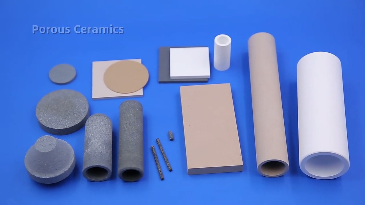
Overview of Porous Ceramics
When it comes to microporous ceramics, the porous ceramics must be explained first.Porous ceramic is a new type of ceramic material, also known as porous functional ceramic. It is a ceramic material with a large number of open or closed pores. It is made by calcining at high temperatures, and many porous structures are made during the sintering process.
Classification of Porous Ceramics
Porous ceramics can be classified by dimension, phase composition, and pore structure (pore size, pore morphology, and pore connectivity), among others.The pore structure can be divided into uniform pore structure and non-uniform pore structure.According to the pore-forming method and pore structure, it can be divided intothe intergranular ceramic sintered body (ie, microporous ceramics), foamed ceramics, and honeycomb ceramics.
According to the size of the pore size, Microporous ceramics is divided into as below:
| Type | Pore size |
| Coarse pores | >500μm |
| Large pores | 100~500μm |
| Micro pores | 1~100μm |
| Nanopores | <1um |
Definition of Microporous Ceramics
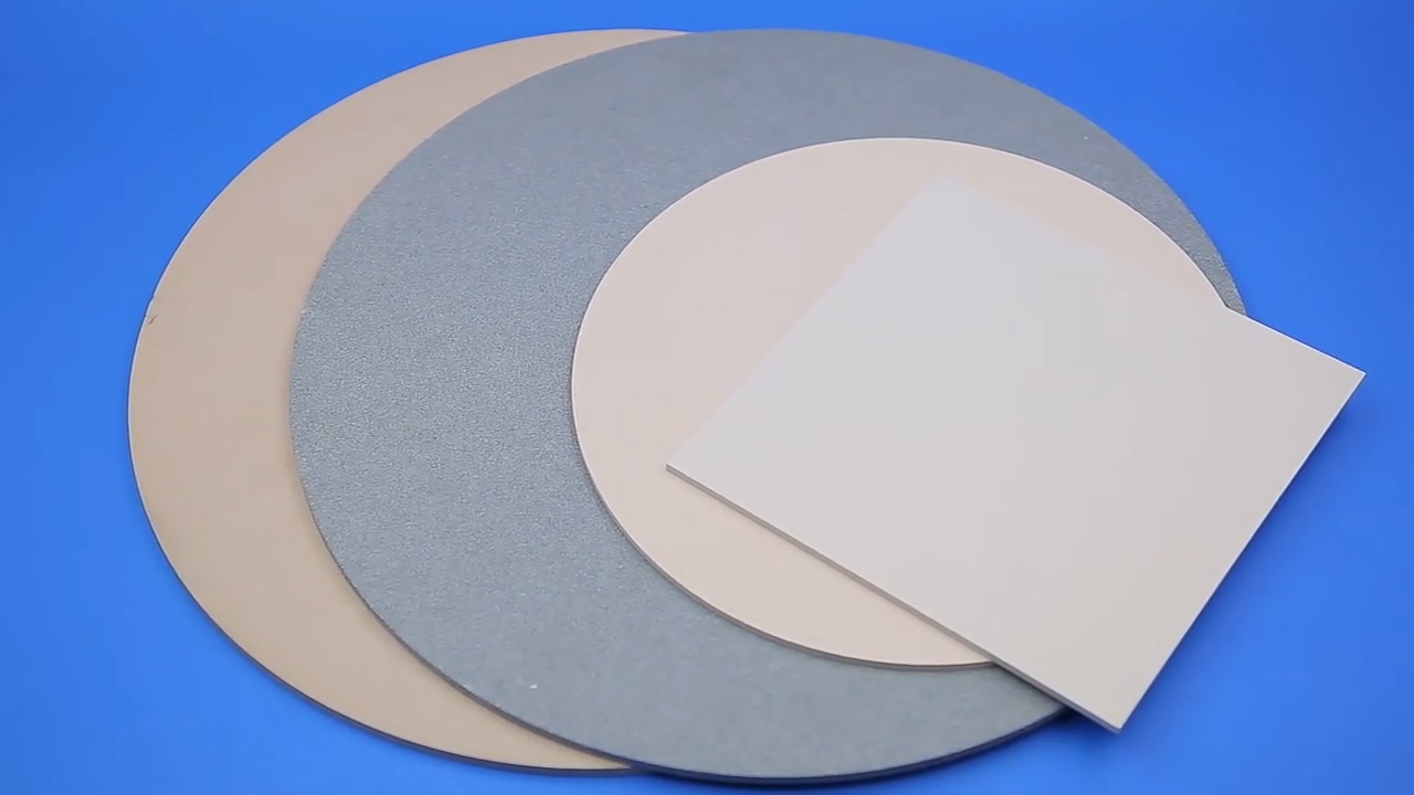
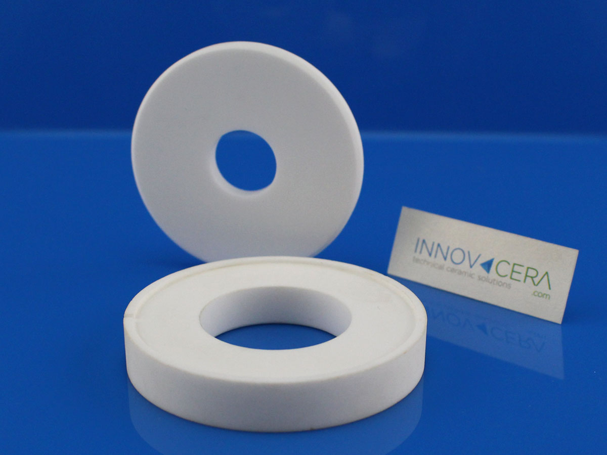
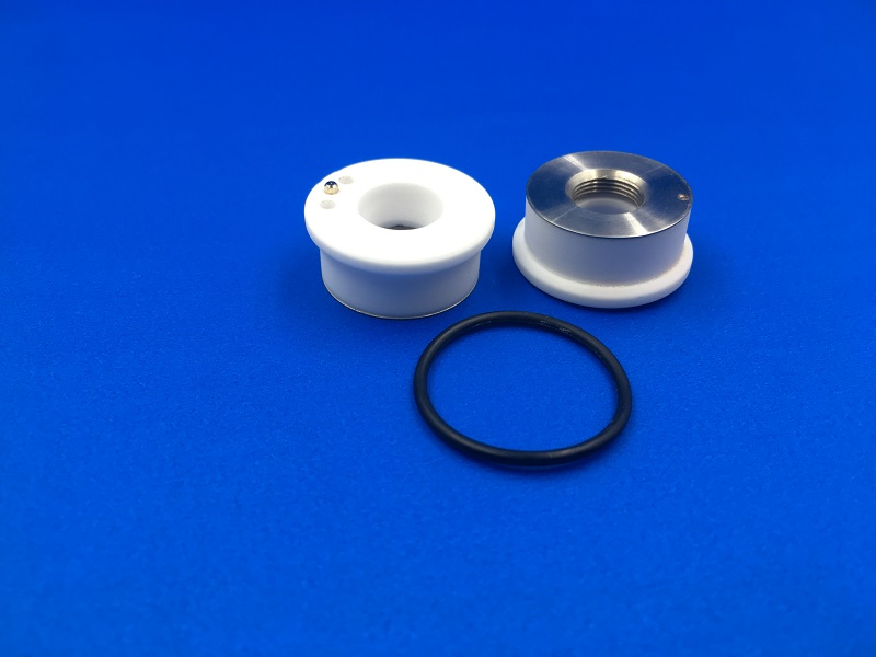
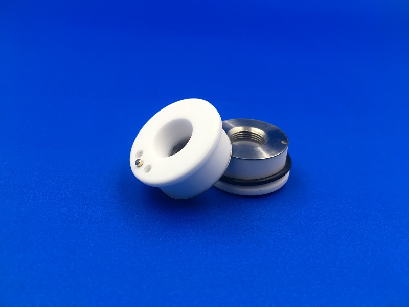
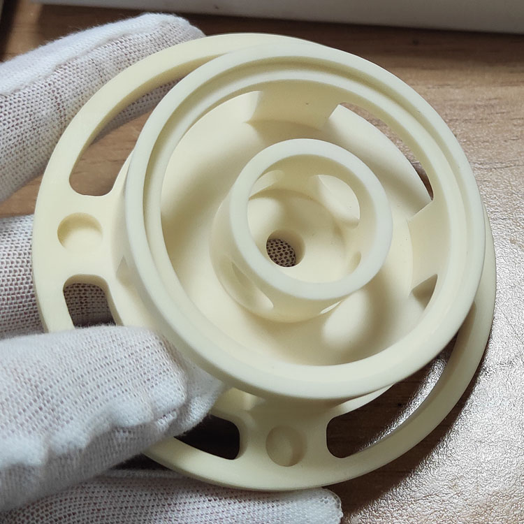
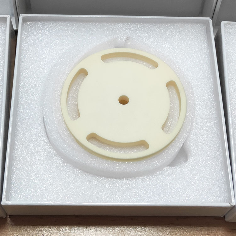
Microporous ceramics have a uniform pore structure, which is a new type of functional structural ceramics. The micropores are very small and are generally micron or submicron, which is invisible to the naked eye. However, microporous ceramics are visible in daily life, such as the ceramic filter elements used in water purifiers and the atomizing cores in electronic cigarettes, etc.
Fabrication of Microporous Ceramics
Porous ceramic pore-forming principles and methods mainly include as below.
Particle accumulation→ Addition of pore agents→low-temperature underfired →mechanical processing into pores.
Asa new type of inorganic non-metallic filter material, microporous ceramics are made of aggregate particles mixed with a certain amount of binder, and then fired at high temperature after the pore-forming agent.
Quartz sand, corundum, alumina (Al2O3), silicon carbide (SiC), mullite (2Al2O3-3SiO2), and ceramic particles are used as aggregates. Generally, aggregates are required to have high strength, heat resistance, corrosion resistance, close to spherical shape (easy to construct into filtration conditions), easy granulation within the specified particle size range, and good affinity with binders. If the aggregate base material and particle size are the same, and other conditions are the same, the pore size, porosity, air permeability and other indicators can achieve the ideal purpose.
Application of Microporous Ceramics
Microporous ceramics have the advantages of adsorption, gas permeability, corrosion resistance, environmental compatibility, biocompatibility, surface structure with unique physical and chemical properties, etc.
As gas-liquid filtration, purification and separation, gas distribution, sound absorption, and shock absorption, heat exchanger materials and chemical fillers, bioceramics and catalyst carriers, adsorbents, biological implant materials, special wall materials, artificially manufactured organs, and refractory materials, sensor materials, etc.
Silicon carbide porous ceramics have been widely used in environmental protection, energy saving, aerospace, chemical, petroleum, smelting, food, pharmaceutical, biological, medical, aquaculture, and other industries, greatly improving the product quality and market competitiveness of these industries.
Silicon Carbide Porous Ceramics
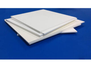
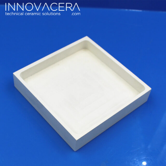
Alumina Porous Ceramics

 Enquiry