As data center networks continue to evolve toward higher bandwidth, optical modules are advancing from 800G to 1.6T. Higher transmission rates typically come with increased device integration and more complex packaging designs, posing new challenges for thermal management within the modules. Power consumption levels vary across different 1.6T products due to factors such as DSPs, lasers, packaging architecture, and application scenarios, making it impossible to represent all products with a single power figure. However, as device density and power density increase, establishing stable and efficient thermal pathways has become a critical consideration in next-generation optical module design.
For optical modules, heat dissipation is not solely dependent on external heat sinks. Heat generated by sources such as lasers, modulators, and driver chips must be transferred step by step through the chip mounting structure, substrate, interface materials, and downstream cooling structures. If heat transfer is impeded at any stage, localized temperature rise may occur. Therefore, as 1.6T optical modules move toward higher integration, the thermal performance, dimensional accuracy, and processing quality of ceramic substrates have become increasingly important considerations..
1. Where Do the Thermal Challenges of 1.6T Optical Modules Come From?
The main challenge in thermal management for 1.6T optical modules stems from increasingly concentrated heat sources within a limited space. Inside an optical module, laser diodes, optoelectronic components, driver circuits, and high-speed signal processors are typically integrated. As device performance and integration density improve, multiple heat sources become concentrated within a confined package area, placing higher demands on internal heat dissipation.
At the same time, the structural space available for heat dissipation within the optical module itself is limited. Heat must be transferred step by step through paths such as chips, bonding layers, substrates, and metal structures to reach the final heat sink. Consequently, thermal resistance at different material layers and interfaces along this path significantly affects overall cooling efficiency.
For 1.6T optical modules, thermal design cannot rely solely on downstream heat dissipation capabilities; it also requires minimizing thermal resistance between heat-generating components and the heat-dissipating structure. The substrate, as a key component, must have its material and structure carefully considered within the overall thermal management design.
2. Why Is AlN Suitable for Thermal Management in High-Speed Optical Modules?
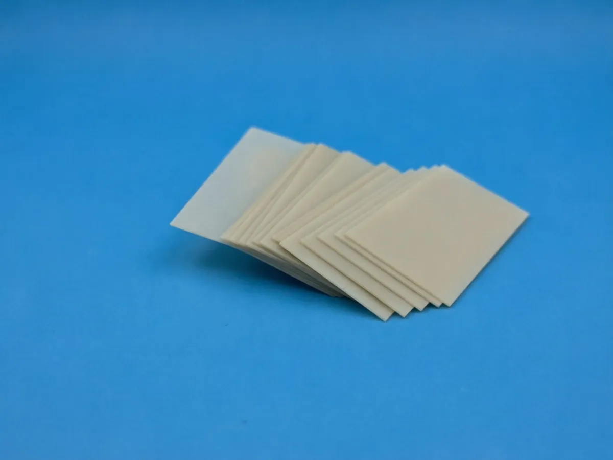
Aluminum nitride (AlN) ceramic has attracted attention in optoelectronic packaging primarily because it combines high thermal conductivity with excellent electrical insulation within a single material.
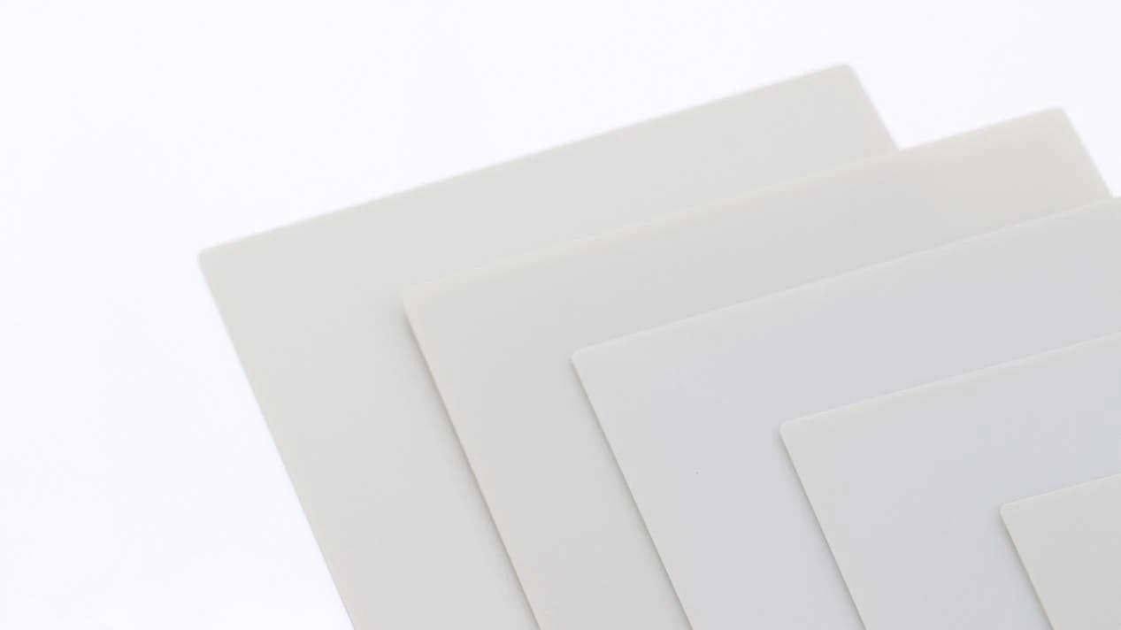
In chip packaging structures, the substrate not only provides mechanical support but may also need to facilitate heat transfer to downstream thermal dissipation components while maintaining necessary electrical insulation. AlN, with its high thermal conductivity and excellent electrical insulation, can provide an effective thermal conduction path while maintaining electrical isolation.
Additionally, AlN features a low coefficient of thermal expansion, which helps reduce thermal expansion mismatch when combined with silicon, metals, and other packaging materials. However, the thermal conductivity, electrical, and mechanical properties of different AlN materials can vary depending on factors such as composition, density, and manufacturing processes. Therefore, in engineering applications, specific material grades and supplier data must be carefully evaluated and confirmed.
3. Thermal Conductivity Is Not the Only Criterion for AlN Substrate Selection
For high-integration packages like 1.6T optical modules, merely relying on the thermal conductivity of AlN is not sufficient to determine whether a substrate is suitable for practical application. Even when the same AlN material is used, changes in substrate thickness will affect the thermal resistance through the substrate. Significant warpage, thickness variation, or unsuitable surface conditions may also affect chip mounting, metallization, and interface contact, ultimately affecting packaging performance.
The selection of the AlN substrate requires consideration of material properties, size, and processing quality simultaneously:
| Key Parameter | Impact on Practical Applications |
|---|---|
| AlN material grade | Affects thermal performance, electrical insulation, and material consistency |
| Thermal conductivity and test conditions | Used to evaluate the thermal conduction capability of the substrate itself |
| Substrate thickness and tolerance | Affects thermal resistance, structural support, and package space |
| Flatness/warpage | Affects chip mounting and interface contact |
| Surface roughness | Related to mounting, metallization, and interface quality |
| Dimensions and machining tolerances | Must match the specific packaging structure |
| Surface and edge quality | Affects subsequent processing and assembly quality |
| Batch‑to‑batch consistency | Affects process stability during volume production |
Therefore, high thermal conductivity is only one of the basic indicators for selecting AlN substrates. In practical applications, it is necessary to make a comprehensive judgment by considering factors such as size accuracy, surface condition, and subsequent processing requirements.
4. How Does AlN Substrate Thickness Affect Heat Dissipation in the Package?
Substrate thickness is often overlooked in package design, yet it can have a significant impact on the thermal path. From a heat transfer perspective, under conditions where the material thermal conductivity and heat transfer area are similar, an increase in substrate thickness will lead to an increase in the thermal resistance in the thickness direction. Therefore, using a thinner substrate can shorten the heat transfer distance in the thickness direction, thereby reducing the thermal resistance of the substrate in that direction and also helping to reduce the space occupied by the package.
However, this does not mean that the thinner the AlN substrate, the better. As the thickness decreases, the mechanical rigidity, processing stability, and risk of damage during assembly also need to be re-evaluated; a thicker substrate can provide better structural support, but at the same time, it will increase the heat transfer distance in the thickness direction and occupy more package space.
Therefore, 0.635 mm, 1.0 mm, or other thickness specifications cannot simply be defined as the “best” thickness for 1.6T optical modules. The actual selection should consider chip size, heat load, heat transfer area, package space, interface materials, mechanical support requirements, and subsequent processing requirements. For specific projects, a more reasonable approach is to first clarify the package structure and the target heat path, and then determine the size, thickness, and processing tolerance required for the AlN substrate.
5. From Material Selection to Overall Thermal Path Design
For the next-generation high-speed optical modules, the real issue to be addressed is not whether “AlN can dissipate heat”, but whether the selected AlN substrate can form an effective and stable thermal transfer path with the entire packaging structure.
The heat generated by the chip needs to pass through multiple stages such as the interconnect layer, substrate, interface material, and downstream cooling structure before being ultimately transferred out. If the substrate itself has good thermal properties, but the interface thermal resistance between the chip and the substrate is high, or there are contact issues between the substrate and the downstream cooling structure, even if a higher thermal conductivity AlN is used, the final heat dissipation effect may still be limited.
Therefore, during the development of 1.6T optical modules, the evaluation of the AlN substrate needs to go beyond the single material performance and extend to the entire packaging thermal path. In addition to thermal conductivity, the evaluation should also take into account the substrate size, thickness, flatness, surface condition, interface material, and compatibility with other packaging materials.
Rather than simply seeking AlN with higher thermal conductivity, it is more effective to define the target thermal path at the early stage of the project and then determine the required material properties, dimensional accuracy, and processing specifications for the AlN substrate.
6. INNOVACERA AlN Ceramic Substrate
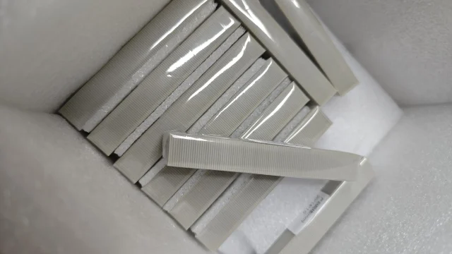
INNOVACERA provides different specifications of AlN ceramic substrates and related precision ceramic products, which can be used for optoelectronic devices, high-power electronic packaging, and other applications requiring good thermal conductivity and electrical insulation. The substrates can be supplied in different sizes, thicknesses, dimensional tolerances, and surface finishes according to specific project requirements, and the specifications can be evaluated in combination with subsequent metallization, mounting, or packaging processes.
For 1.6T optical modules and other high-speed optoelectronic packaging projects, if you are evaluating AlN substrates, you can provide information on chip size, substrate dimensions, thickness requirements, thermal conductivity requirements, flatness and surface requirements, and subsequent processing conditions. This information can be used to evaluate suitable AlN material grades and substrate specifications.
For more details, please contact sales@innovacera.com.