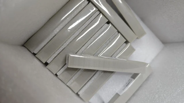
As the demand for high-speed interconnects in AI data centers continues to grow, 800G optical modules have become a key product form in high-bandwidth data center networks. Compared with earlier-generation lower-speed optical modules, 800G modules must support significantly higher data rates within a similarly limited packaging space, while also facing greater power consumption and thermal management challenges. Some commercial products already consume up to ten watts of power, with actual levels varying depending on product architecture, transmission distance, and component configuration.
For module design, the impact of increased data rates extends beyond mere processing capability. Lasers, optoelectronic components, driver chips, and signal processors must be integrated at higher densities within confined spaces, leading to localized heat accumulation. Effectively dissipating this heat while maintaining necessary electrical insulation and structural stability during cooling has become a critical challenge in 800G optical module packaging design.
With these advanced design requirements, substrate materials are no longer only responsible for mechanical support. They also need to conduct heat efficiently, ensure electrical insulation, and maintain proper thermal expansion matching. Aluminum nitride (AlN) ceramics feature high thermal conductivity, reliable insulation performance and a relatively low thermal expansion coefficient. For this reason, AlN is widely favored as a substrate material for high-heat-flux electronic and optoelectronic packaging.
1. Why is thermal management capability of the substrate more critical for 800G optical modules?
800G optical modules must perform high-speed optoelectronic conversion and signal processing within a limited form factor, requiring heat generated by chips and other components to be efficiently transferred through the packaging structure to downstream heat dissipation paths.
Failure to effectively dissipate localized heat will cause obvious temperature gradients, making it harder to stabilize device temperature. In addition, optoelectronic packaging adopts a multi-material system, including semiconductor chips, metal frames, connecting materials and ceramic substrates. When operating temperature fluctuates, mismatched thermal expansion between these different materials generates residual stress at the bonding interfaces.
Therefore, the ceramic substrate in 800G optical modules should not be evaluated solely based on its insulation properties, but must instead be assessed comprehensively considering:
| Design Requirement | Substrate‑Related Properties to Consider |
|---|---|
| Heat Dissipation for Chips & Components | Thermal Conductivity and Heat Conduction Path |
| Electrical Isolation | Insulation Performance |
| Temperature Variation and Thermal Cycling | Coefficient of Thermal Expansion and Structural Stability |
| Precision Packaging | Dimension, Thickness and Flatness |
| Interface Bonding | Surface Roughness and Cleanliness |
| Mass Production | Consistency of Material and Machining Process |
This is also a key reason why AlN is gradually entering the selection range for high-speed optoelectronic packaging materials.
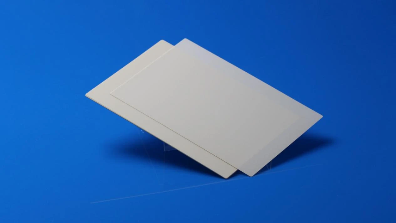
2. Why is AlN suitable as the substrate for high heat flux optical devices?
For 800G optical modules, the substrate needs to address two issues simultaneously: Firstly, the heat generated by the chips and other heat-generating components needs to be promptly transferred to the heat dissipation structure through the substrate; Secondly, the packaging structure needs to maintain necessary electrical insulation. The advantage of AlN ceramics lies in being able to combine these two requirements – providing high thermal conductivity while maintaining insulation, thereby establishing a relatively direct heat dissipation path for the optical devices.
In addition to thermal conductivity and insulation properties, the thermal expansion coefficient of AlN also makes it suitable for multi-material packaging structures. The interior of an optical module typically contains semiconductor chips, metal layers, bonding materials, and ceramic substrates. Different materials expand at different rates under temperature changes. The relatively low thermal expansion coefficient of AlN helps control the thermal expansion mismatch between materials and reduces the interface stress generated during temperature cycling. However, the actual packaging reliability still depends on the material combination and connection method of the entire structure, and cannot be solely determined by the substrate material alone.
Therefore, when choosing an AlN substrate, the focus should not be on “how high the thermal conductivity is”, but rather on confirming the material grade, thermal conductivity guarantee values and testing methods, thermal expansion coefficient, dimensional accuracy and surface condition to ensure they are in line with the specific packaging design. For R&D and procurement teams, these parameters jointly determine whether the AlN substrate can truly match the subsequent packaging process, rather than the higher the single performance indicator, the better.
3. Why can’t one solely rely on thermal conductivity when choosing an AlN substrate?
For high-speed optical modules, thermal conductivity is an important parameter, but it is not the sole criterion for determining whether an AlN substrate is suitable for a project.
After entering the sample verification and mass production stages, the geometric accuracy and surface processing state of the substrate may also affect the stability of the packaging. For instance, thickness deviation, flatness or warping may affect chip mounting and interface contact; surface roughness, scratches, chipping and contaminants need to be controlled in combination with specific bonding, metallization or other subsequent processing techniques.
Therefore, when actually purchasing an AlN substrate, it is recommended to simultaneously confirm the following parameters:
| Key Parameters | Focus Points for Procurement / Verification |
|---|---|
| AlN Material Grade | Thermal‑conductivity grade, test conditions and material consistency |
| Substrate Dimension | Length, width, profile and dimensional tolerance |
| Thickness | Target thickness and thickness tolerance |
| Flatness / Warpage | Compatibility with mounting and subsequent packaging processes |
| Surface Roughness | Determined according to subsequent processes such as bonding and metallization |
| Surface Quality | Defect control for chipping, scratches, contamination and others |
| Batch‑to‑batch Consistency | Stability of dimension, thickness and material properties |
For mass production projects, the fact that a single sample achieves high performance indicators does not necessarily mean that subsequent batches will maintain the same level. Whether the material properties, dimensional accuracy, and surface processing quality can remain consistently stable is also an important aspect of research and development verification as well as supplier assessment.
4. What thickness should be chosen for the AlN substrate of the 800G optical module?
There is no uniform “optimal AlN substrate thickness” for 800G optical modules. The actual thickness needs to be determined based on the chip size, installation space, heat conduction path, mechanical support requirements, and subsequent packaging process.
A thinner AlN substrate can shorten the heat conduction path in the thickness direction and is conducive to the design of compact packaging structures. However, it is also necessary to consider mechanical strength, damage during processing, and warping risks.
Increasing the substrate thickness can improve the structural rigidity to a certain extent, but it will also change the heat conduction path and the packaging space. Therefore, thicknesses such as 0.25 mm, 0.38 mm, 0.635 mm, and 1.0 mm can all be considered as candidate specifications for specific projects, and a single thickness should not be simply defined as suitable for all 800G optical modules.
A more reasonable selection method is to first clarify the packaging structure and thermal design requirements, and then determine the size, thickness, tolerance, flatness, and surface condition of the AlN substrate.
5. INNOVACERA AlN Ceramic Substrates Supply
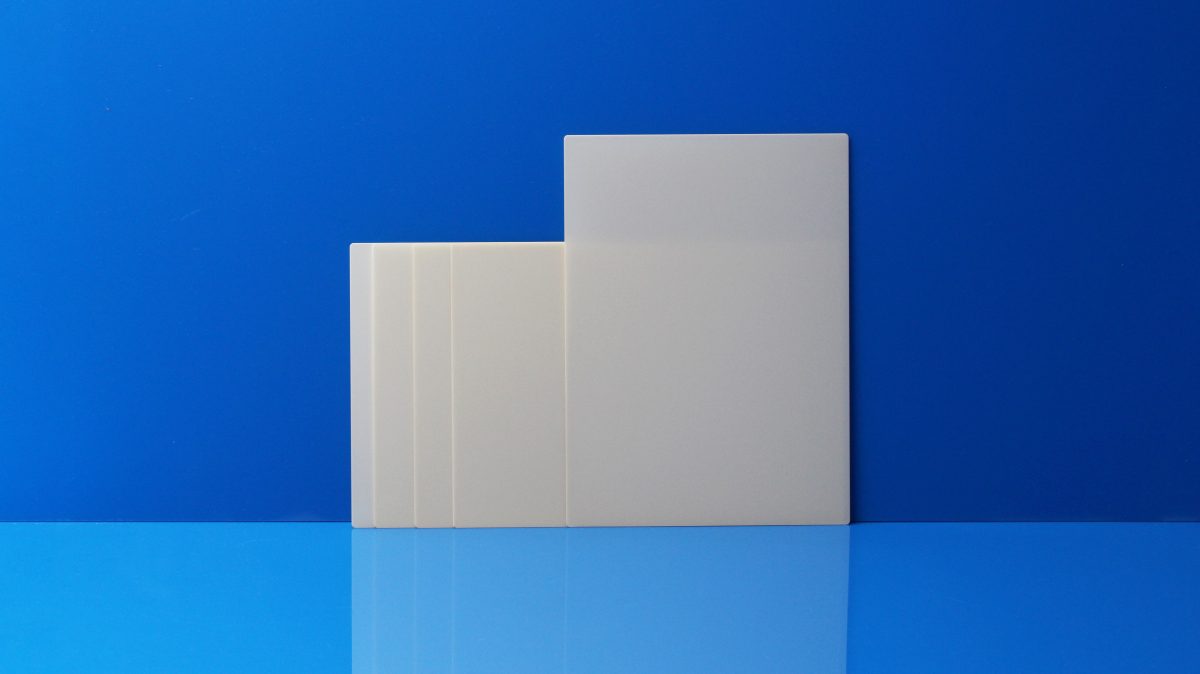
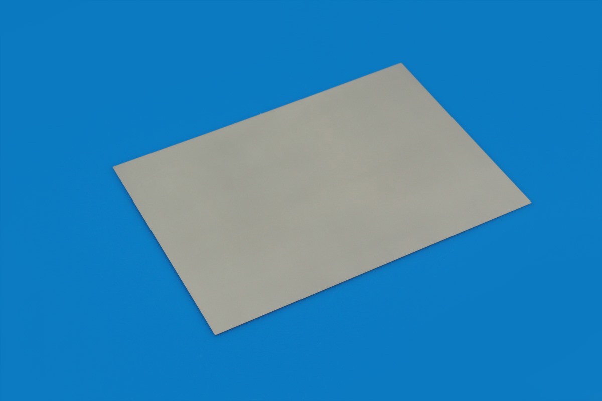
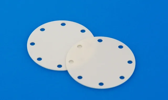
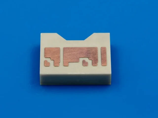
INNOVACERA can provide Aluminum nitride (ALN) Substrates for high-speed optical modules, photonic packaging, and related electronic devices. These substrates are available in various sizes and thicknesses, with surface finishing options available according to application requirements.
If you are selecting substrates for 800G optical modules or other high-speed photonic packaging projects, please provide parameters such as substrate size, target thickness, thermal management requirements, flatness, and subsequent processing techniques. INNOVACERA can assist in matching suitable AlN ceramic substrate specifications based on specific application needs and provide samples and custom processing support. For details, please contact sales@innovacera.com.