Innovacera a leading supplier of advanced ceramic components and solutions for the semiconductor and electronics industry, is excited to announce its participation in a foreign exhibition, one of the important events in the semiconductor and microelectronics industry.
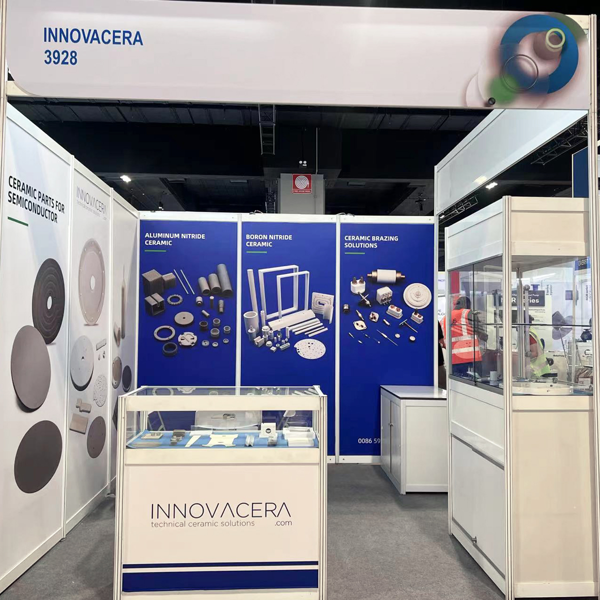
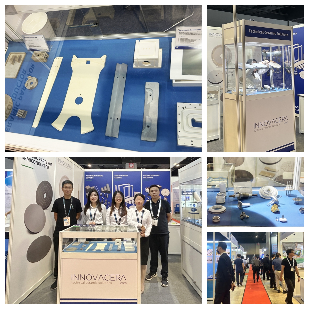
Innovacera is showcasing its latest advancements in technical ceramic solutions in the semiconductor industry. Attendees can visit us at Booth 3928, where we are presenting:
- Ceramic to Metal Sealing Product: Including the metalized ceramics, AMB, DPC, and DBC substrates which are widely used for electrical packaging processes, high-power semiconductor packaging, semiconductor cooling, and UPS uninterruptible power supply, photovoltaics, high-speed railway, new energy vehicle, high voltage network, and communication.
- Boron Nitride components: essential for various high-tech applications, including electrode insulation for vacuum high-temperature equipment, PVD/CVD vacuum coating equipment insulation accessories, ion coating machines, sputtering coating, semiconductor MOCVD equipment for insulation and heat dissipation, ion implanter insulation accessories, PBN VGF crucibles, LEC crucibles, MBE crucibles, and PBN ceramic boats. These BN ceramics offer significant advantages such as high-temperature resistance up to 2000℃, thermal shock resistance, high electrical breakdown strength (3-4 times that of alumina), and superior carbon atmosphere corrosion resistance compared to alumina. Additionally, they exhibit large resistance, high-temperature resistance, high electrical breakdown resistance, no pollution, corrosion resistance, and machinability, making them ideal for demanding industrial environments.
- High Purity Alumina Ceramic Part: Such as alumina polishing plates and turn tables which are polished surfaces and high precision flatness, high rigidity, high chemical durability, and ultra-large size are some of our advantages.
INNOVACERA ATTEND THE SEMICON SEA 2024 EXHIBITION
Engineered technical ceramics are widely used in the semiconductor manufacturing process due to their high-temperature stability, electrical insulation, corrosion resistance, and excellent mechanical properties. INNOVACERA ultra-pure ceramics are used in the whole-cycle semiconductor manufacturing process including wafer manufacturing, device manufacturing, and packaging.
As the semiconductor industry continues to evolve rapidly, the exhibition provides an essential chance for industry stakeholders to stay ahead of technological advancements and market trends. Whether you’re an industry veteran or a newcomer, the event offers unparalleled opportunities to gain insights, network with peers, and explore the future of the semiconductor landscape. This event is essential for driving the growth and development of the semiconductor ecosystem.
For more information about Innovacera products and exhibitions arranged, welcome to contact us at sales@innovacera.com.
Declaration: This is an original article of INNOVACERA®. Please indicate the source link when reprinting: https://www.innovacera.com/news/innovacera-is-on-attending-the-foreign-exhibition.html.


 Enquiry