.svg)
Technical Ceramic Components are integral to semiconductor manufacturing equipment, technical ceramic components are high in purity with low levels of trace metals, this means they can constitute either the process chamber material or interior process surfaces for CVD, PVD, plasma etching, and ion implanting where their strong dielectric properties are highly beneficial, so it is widely used in the semiconductor industry.
 The semiconductor industry uses advanced technical ceramics including alumina ceramic (AL2O3), aluminum nitride (ALN), Porous Ceramic, Boron Nitride (BN), pyrolytic boron nitride (PBN), and silicon carbide (SiC). PBN has primarily been used for crucibles in metal oxide (MOCVD) deposition tools, the mainly single crystal growth methods are LEC and VGF, so PBN LEC and VGF crucibles are required. PBN molecular beam epitaxy (MBE) crucibles are one of the most important epitaxy growth processes for group III-V and group II-VI semiconductor crystals in the world today. PBN crucible is the best container for evaporating elements and synthetic materials in this process. The PBN ring around the evaporation crucible is used in OLED equipment.
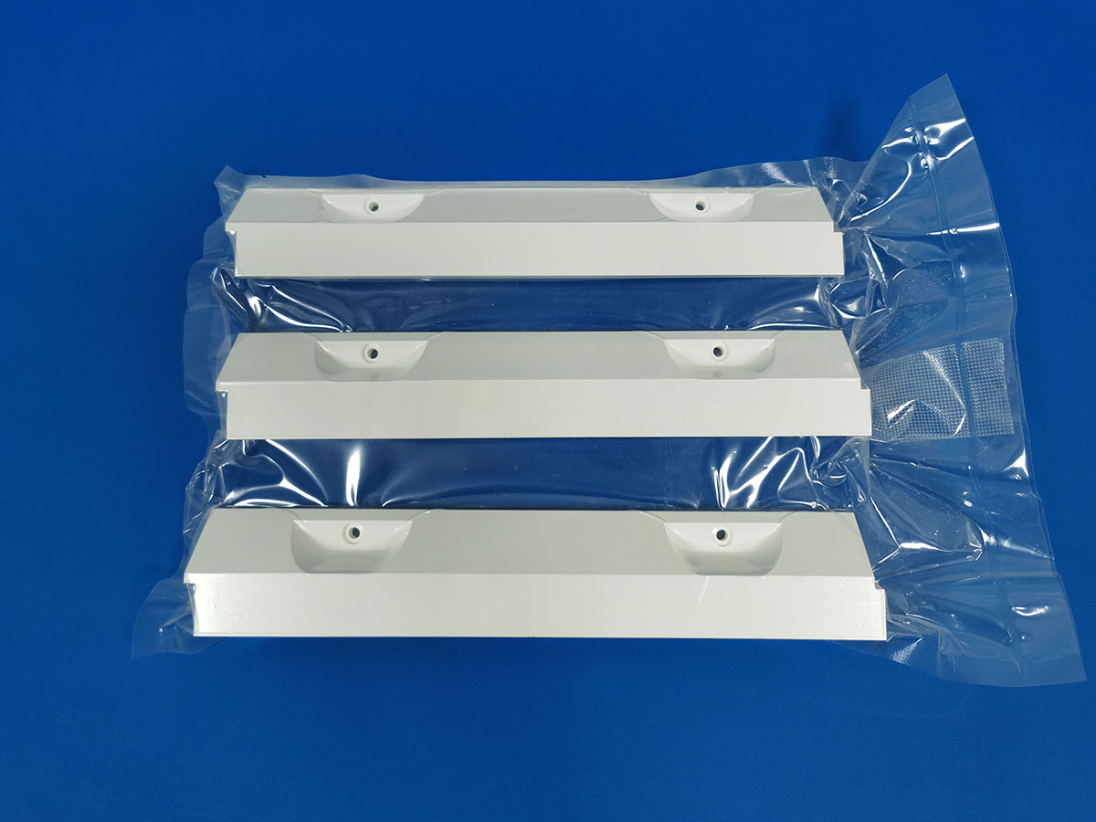
More ceramic parts used for the semiconductor industry are as below:
 |
 |
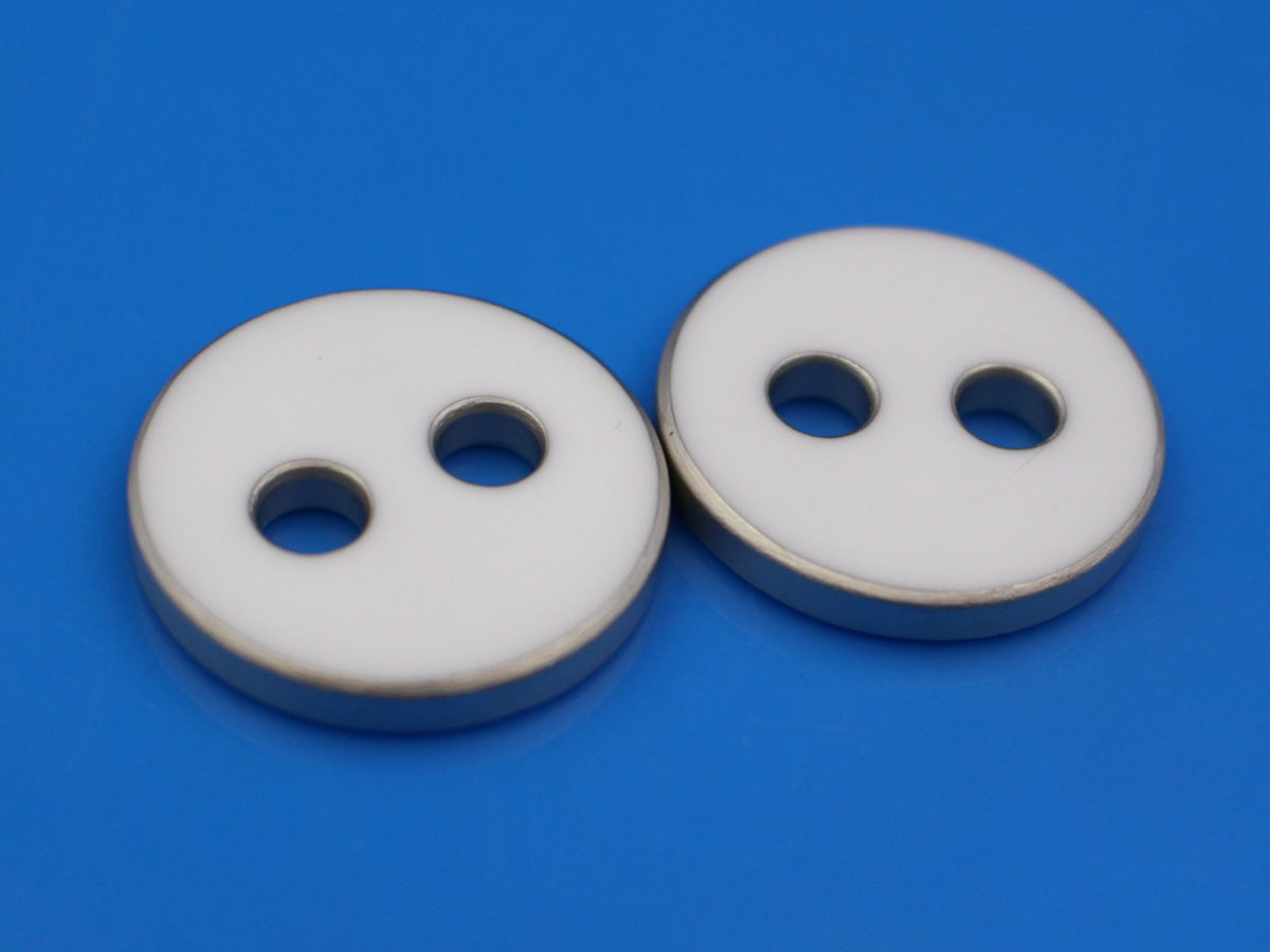 |
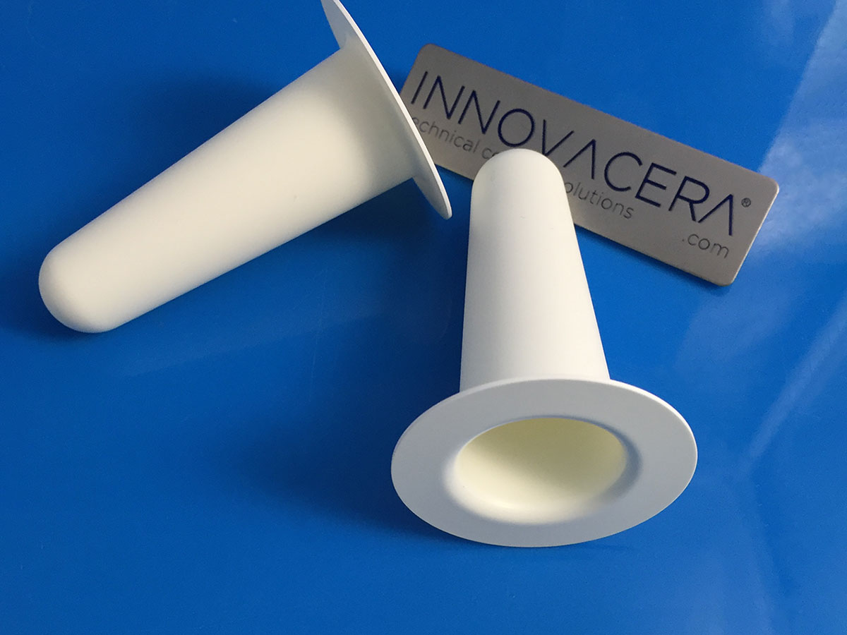
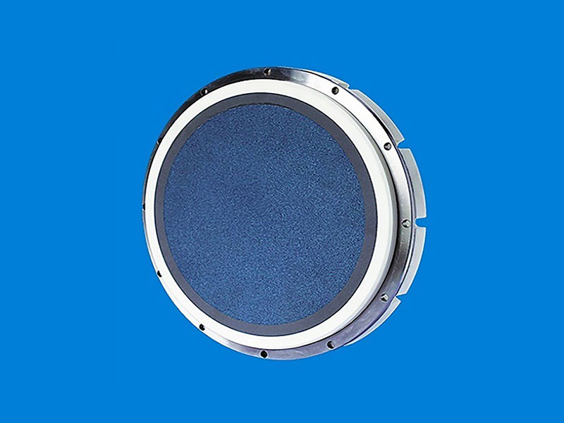
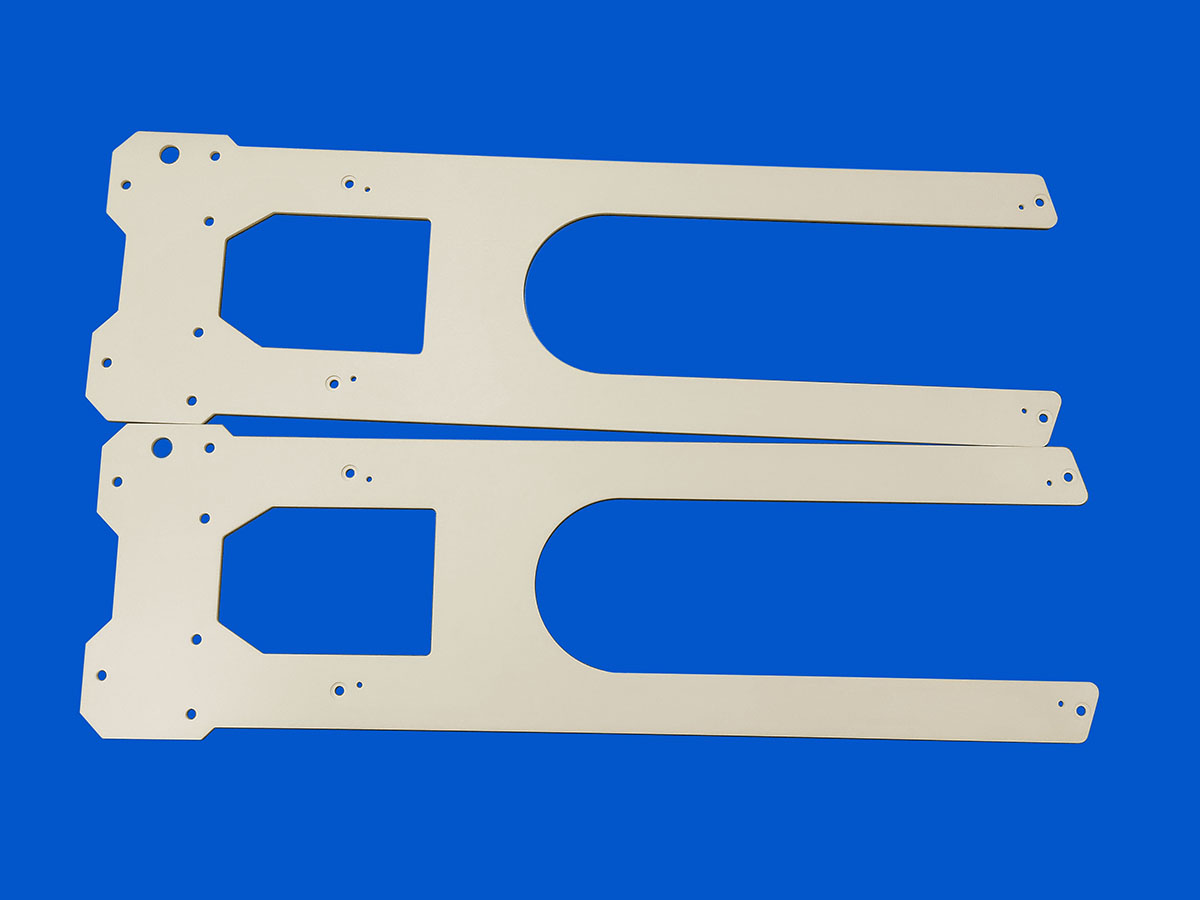
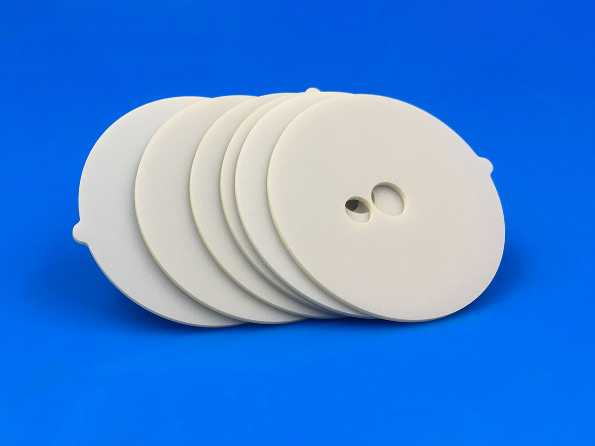
| Boron nitride ceramic insulator part used for PVD and MOCVD equipment. | Porous ceramics are widely used for Vacuum chucks. | Metallized ceramic parts for IC package. |
 Alumina ceramic and aluminum nitride are typically used for electrostatic chucks in chamber interiors. Innovacera manufacture ceramic wafer (generally called robot’s hand) which is used for end effectors, ceramic end effectors have good stiffness and high strength, so the robot arm settles to its final position faster. End effectors constitute the end of the robot arm which handles and moves the semiconductor wafer between positions.
The ceramic material is chosen based on the deposition chemistry to which it will be exposed. Such as if plasma is used, a minimum of 99.5% alumina must be used. Plasma corrosion resistance is the main characteristic of components in semiconductor manufacturing equipment.
 Aluminum nitride (AlN) is a covalent bond compound with a hexagonal wurtzite structure with lattice parameters a=3.114 and c=4.986. The color usually is gray and is a typical III-V wide-bandgap semiconductor material.
Aluminum nitride ceramics have the characteristics of high strength, high volume resistivity, high insulation withstand voltage, thermal expansion coefficient, and good matching with silicon. They are very suitable for semiconductor substrates, ceramic electronic substrates, and structural packaging materials. The potential in the electronics industry is huge.
Innovacera is an advanced ceramic components manufacturer established in 2012, has rich experience in the ceramic industry, strictly controls the product quality and inspection by excellent teams. We offer custom solutions beyond our existing products. We warmly welcome customers to establish cooperation and create a bright future with us together.
For more information, please contact us as below:
A506-507, No.7 Yu’nan Fourth Road, Huli District, Xiamen, Fujian, China
Tel: 86-592-5589730
Email: sales@innovacera.com
Website: www.innovacera.com
Declaration: This is an original article of INNOVACERA®. Please indicate the source link when reprinting: https://www.innovacera.com/news/semiconductor-ceramic-components.html.


 Enquiry