As consumer electronics, automotive electronics, new energy systems, and communication equipment continue to evolve toward miniaturization, higher power density, and greater reliability, electronic components must operate stably under increasingly compact PCB spaces, elevated operating temperatures, and automated surface-mount assembly processes.
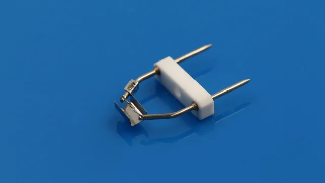
Surface-mounted fuses (SMD fuses) are common overcurrent protection devices in electronic circuits. When a circuit experiences abnormal overload or short-circuit conditions, the fusible element within the fuse melts and opens the circuit, thereby reducing the risk of damage to downstream circuits and critical electronic components caused by excessive current.
For SMD fuses utilizing independent ceramic bases or ceramic carrier structures, in addition to the fusible element itself, the ceramic base—which supports the fuse wire, provides electrical insulation, and enables electrode connections—also significantly impacts the device’s manufacturing consistency and long-term reliability.
Alumina ceramics, with their excellent electrical insulation, thermal resistance, mechanical strength, and dimensional stability, combined with mature metallization techniques, have become valuable substrate materials for such electronic protection devices. So why is metallized alumina ceramic suitable for SMD fuse packaging? What are the key structural and process requirements involved?
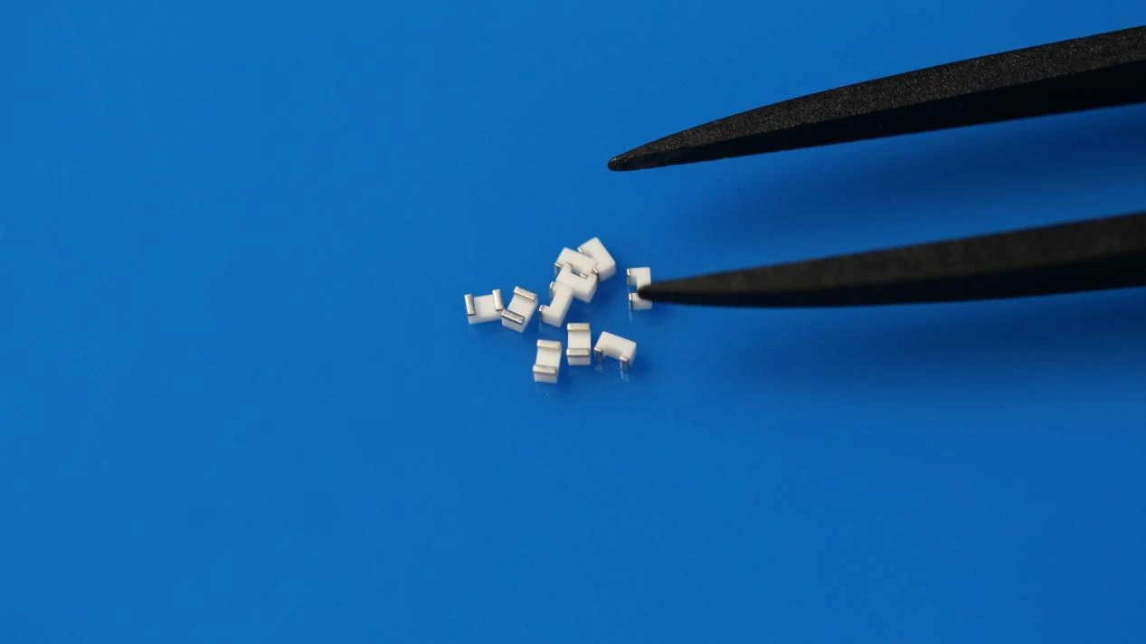
I. What role does the ceramic base play in SMD fuses?
For SMD fuses using a separate ceramic base, the ceramic base is not merely a simple “housing,” but rather a structural component that simultaneously provides insulation, support, positioning, and electrical connectivity.
1. Providing stable electrical insulation
During normal operation and fault-triggered fusing, fuses must sustain reliable insulation between internal conductive components. Alumina ceramic possesses superior electrical insulation and dielectric properties, making it an ideal insulating medium between fuse elements and other conductive structures. For miniature SMD fuses with constrained internal space, rational layout of insulation and metallized areas is especially critical.
2. Offering mechanical support and positioning for the fusible element
Grooved, recessed and other customized ceramic structures provide stable positioning for fusible elements, securing accurate alignment during assembly. Since fusible elements vary in size and configuration across different fuse models, the ceramic base’s width, depth, length and end structure are typically customized to meet specific product specifications.
3. Serving as a foundation for electrode connections
Alumina ceramic itself is an insulating material and cannot directly conduct electricity. Therefore, for fuse designs requiring electrodes on the ceramic surface, conductive layers are typically formed via thick-film metallization processes in designated areas. This enables integration between the insulating ceramic substrate, electrode connections, fusible element assembly, and subsequent packaging procedures.
II. Why Choose 95% Alumina Ceramic as the Fuse Base?
Alumina ceramics are available in multiple purity grades, including 95%, 96%, and 99%. Material selection is determined by balancing electrical performance, mechanical properties, process adaptability, long-term reliability and cost.
For some SMD fuses that use independent ceramic bases, 95% alumina ceramics have a mature material and processing foundation, which can achieve a good balance between performance and cost, and thus have high application value.
1. Excellent electrical insulation performance
The fuse needs to maintain reliable insulation both during normal operation and in the event of a fault. 95% alumina ceramics have good resistivity and dielectric properties, which can meet the basic insulation requirements of electronic protection devices.
At the same time, the ceramic base can form clear insulation areas according to the product structure, providing reliable isolation between the fuse, electrodes, and other conductive components.
2. Excellent thermal stability and dimensional stability
When the fuse melts, the melting area will undergo rapid temperature rise and thermal changes. Therefore, the base material needs to have good thermal stability.
Compared with some organic insulating materials, alumina ceramics have higher thermal stability and better dimensional stability, and are less likely to soften or undergo significant deformation in short-term high-temperature environments.
The ceramic material itself also has good fire resistance and arc resistance properties, but the breaking capacity and arc resistance performance of the fuse ultimately depend on the fuse material, rated voltage, current, cavity structure, and overall packaging design, and cannot be solely attributed to the ceramic base.
3. Suitable for precise molding and metallization processing
For micro SMD components, the base not only needs to meet material performance requirements but also needs to have good dimensional consistency.
Alumina ceramics can be manufactured into U-shaped, slot-shaped, and other irregular structures through different molding processes, and can then undergo precise processing and thick-film metallization to provide a customized foundation for different sizes and structures of electronic protection devices.
III. Why is metallization a key process for alumina ceramic bases?
Alumina ceramics possess excellent insulating properties, but this also means that their surfaces cannot directly handle the electrical connections required by fuses.
Therefore, for products that need to form electrodes on the surface of the ceramic substrate, it is necessary to build a stable conductive layer in the designated area through ceramic metallization.
The typical process flow can be summarized as:
Alumina ceramic substrate → Thick film printing → Metal layer sintering → Necessary surface treatment → Fuse and subsequent packaging assembly
In this way, insulating areas and conductive electrode areas can be formed on the same ceramic substrate, providing a foundation for subsequent fuse connections and packaging.
1. Thick film printing
First, based on the electrode design, conductive paste is precisely printed in the designated area of the ceramic substrate.
For micro ceramic bases, the position, size, and pattern integrity of the metallization area will affect the subsequent fuse assembly and electrical connection, so it is necessary to pay special attention to:
• Electrode position accuracy;
• Metallization area;
• Printing thickness;
• Pattern integrity;
• Edge quality.
According to product design and subsequent connection process, different thick film conductor systems such as Ag and Ag/Pd can be selected.
2. High-temperature sintering
After thick film printing, it is necessary to conduct sintering according to the specific process requirements of the metal paste to form a stable bond between the metallized layer and the ceramic surface.
The sintering temperatures for different paste systems are not exactly the same. For example, in public research, it can be seen that Ag and Ag-Pd thick film conductors undergo sintering at approximately 850°C. However, the actual production temperature, holding time, and heating and cooling curves need to be determined based on the specific paste formula and process window.
Therefore, a fixed temperature range cannot be regarded as a uniform standard for all Ag/Pd metallization systems.
3. Nickel plating, gold plating, etc. surface treatment
According to the final connection and packaging requirements, the metallized area can also undergo nickel plating, gold plating, etc. surface treatment.
The nickel layer can serve as a protective and barrier layer and improve the adaptability of the metallized area to the subsequent connection process; the gold layer can be selected based on the specific requirements of the product for surface performance, connection reliability, and environmental stability.
Therefore, whether to perform nickel plating, gold plating, and the specific thickness of the plating layer need to be determined in combination with the metallization system and the final assembly process.
IV. U-shaped Ceramic Base and Other Structural Designs
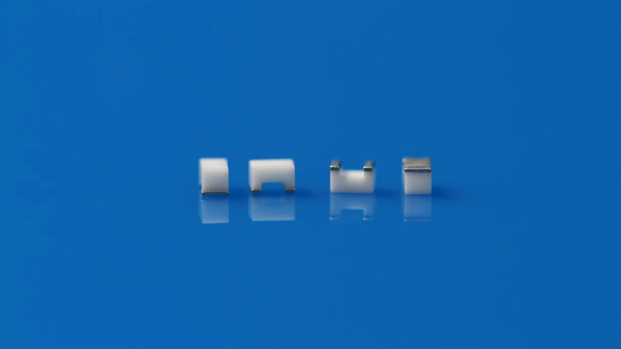
The U-shaped Alumina Ceramic Base is a typical ceramic base structure used in electronic protection devices.
The central groove can provide space for the fuse element to be arranged. The ceramic structures on both sides provide mechanical support and electrical insulation. For specific products, the groove can also help to limit the position of the fuse element, making the internal structure more compact.
However, it should be noted that the U-shaped structure is not the only structural form of SMD fuse ceramic bases, and it does not represent that all fuses are suitable for the U-shaped structure.
Depending on the design of different fuses, the following can also be developed:
• Slot-type ceramic base;
• Concave or localized concave structures;
• Multi-slot or separated slot structures;
• Flat ceramic substrate;
• Other special-shaped ceramic carriers.
The specific structure needs to be designed in combination with the rated current, rated voltage, breaking characteristics, fuse size, internal space and packaging method of the fuse.
For fuses that require larger internal space or higher breaking capacity, the overall packaging structure also needs to comprehensively consider arc control, heat and internal space. Therefore, it cannot be simply judged based on “the U-shaped structure is smaller” regarding its applicability.
V. Key Design and Manufacturing Requirements for SMD Fuse Ceramic Base
For the micro metallized ceramic base, the manufacturing challenges are not just about shaping the ceramic into a certain shape; the more important aspect is ensuring the compatibility among the ceramic size, the metallization quality, and the subsequent assembly process.
1. Ceramic Size Consistency
The overall size of the base, the width of the grooves, the depth, the wall thickness, and the end structure all affect the fuse positioning and subsequent assembly.
During mass production, it is necessary to focus on controlling the size tolerance and batch consistency to avoid assembly deviations or changes in electrical spacing caused by fluctuations in base size.
2. Metallization Position and Adhesion
The metallized area needs to be accurately correspond to the designed electrode position, while ensuring the stable adhesion of the metal layer to reduce the risks of delamination, cracking, etc. during subsequent assembly, welding, and temperature cycling.
For micro ceramic bases, the consistency of the metallization pattern also directly affects the quality of subsequent electrode connection.
3. Fuse and Ceramic Structure Matching
Different SMD fuses have different fuse elements in terms of material, size, and shape, and their selection needs to be determined based on rated current, rated voltage, and fuse characteristics.
Therefore, the width, depth, and positioning structure of the ceramic cavity also need to match the specific fuse element.
4. Matching with Subsequent Packaging Process
The ceramic base is usually only a part of the internal structure of the fuse, and the final product may also combine end electrodes, fuse elements, covers, plastic sealing, or other packaging structures.
Therefore, when designing the ceramic base, it is necessary to confirm in advance:
• Fuse assembly method;
• Electrode connection method;
• Welding or other connection processes;
• Packaging method;
• Surface mount requirements;
• Final reliability requirements.
Different SMD fuses have differences in size, structure, rated parameters, and assembly methods, so the ceramic base can either adopt standard specifications or be adjusted in structure and metallization scheme according to specific product requirements.
VI. Innovacera Metallized Ceramic Customization Service
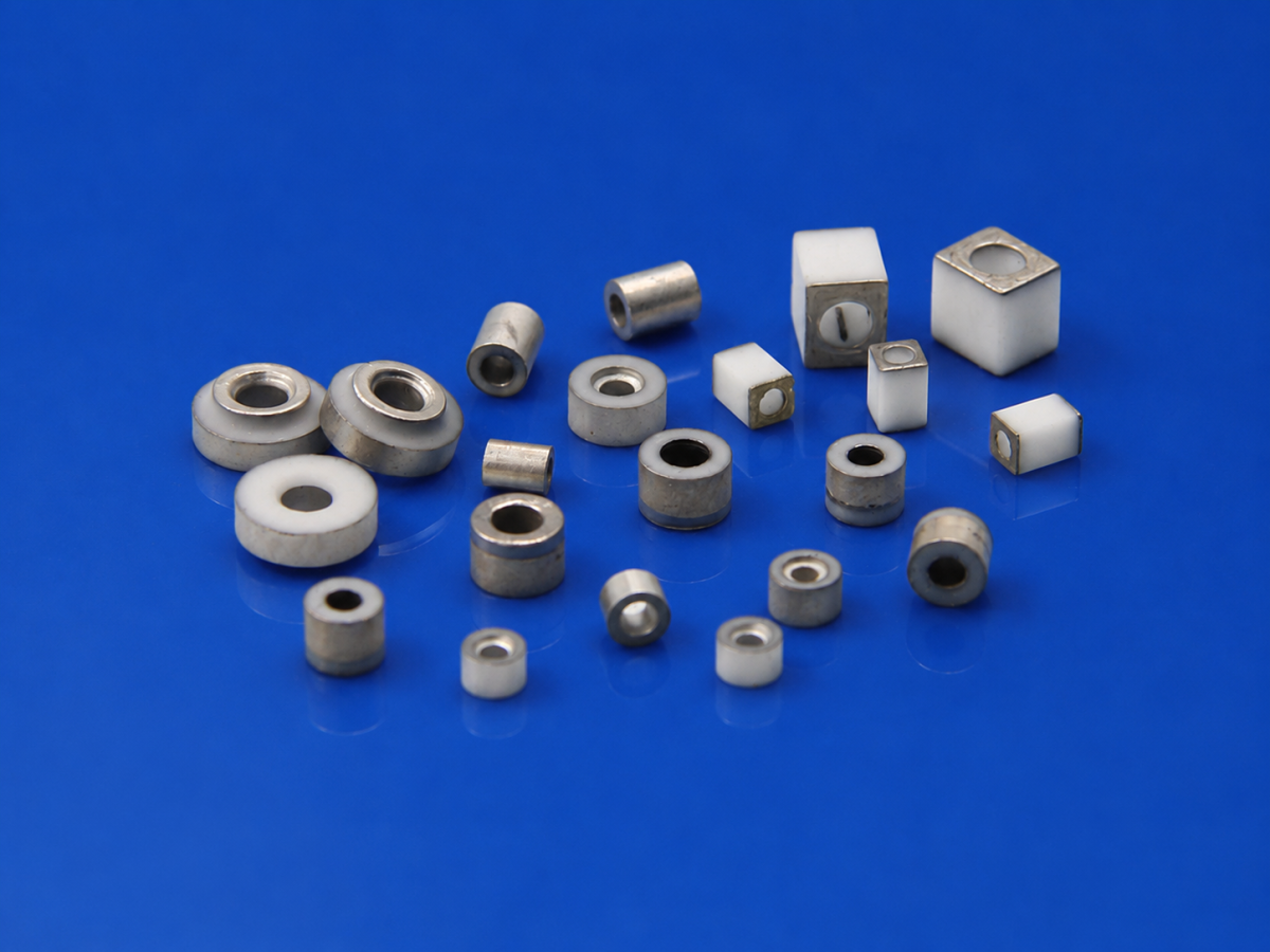
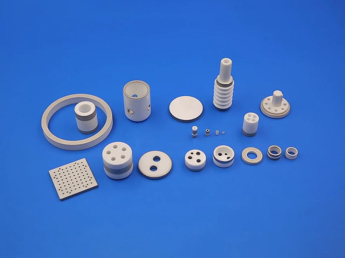
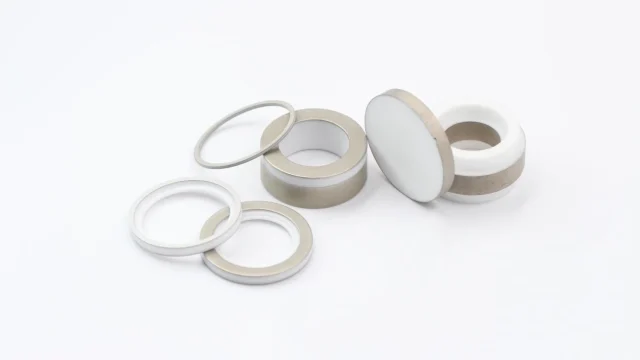
Innovacera provides metallized alumina ceramic components, including SMD fuse ceramic bases and other products. It can offer standard specification products and support customization based on customer drawings, dimensions, and metallization requirements. For U-shaped, slot-shaped, and other irregular structures, corresponding ceramic materials, metallization, and surface treatment schemes can be matched according to specific applications. If you have any product requirements, please feel free to contact us to obtain product specifications, technical support, and quotations.
Email: sales@innovacera.com