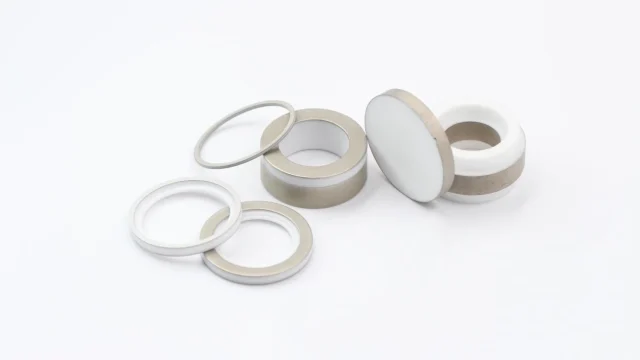
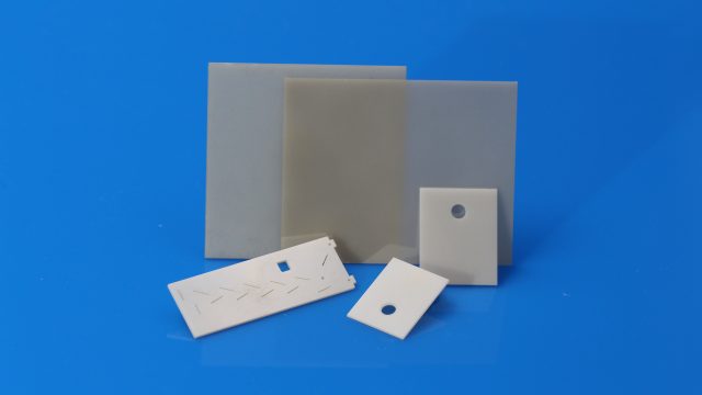
Advanced ceramics are widely used in semiconductor manufacturing process because they combine electrical insulation, thermal performance, chemical and wear resistance, vacuum-process compatibility and dimensional stability. This article Innovacera focuses on four ceramic materials commonly used in semiconductor equipment: boron nitride (BN), alumina (Al₂O₃), aluminum nitride (AlN) and silicon carbide (SiC). Each serves a different engineering function, from electrical insulation and wafer support to vacuum holding and precision motion.
1. Boron Nitride Ceramic Parts for Semiconductor Processing
Hot-pressed boron nitride is widely used in semiconductor processing equipment due to its excellent electrical insulation, high-temperature stability, and machinability, which enables complex geometries and precision-machined components.
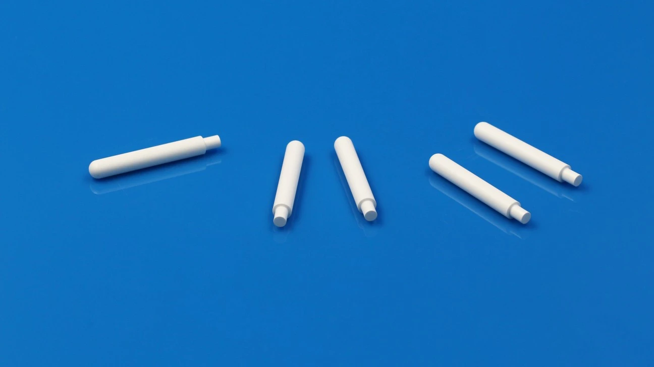
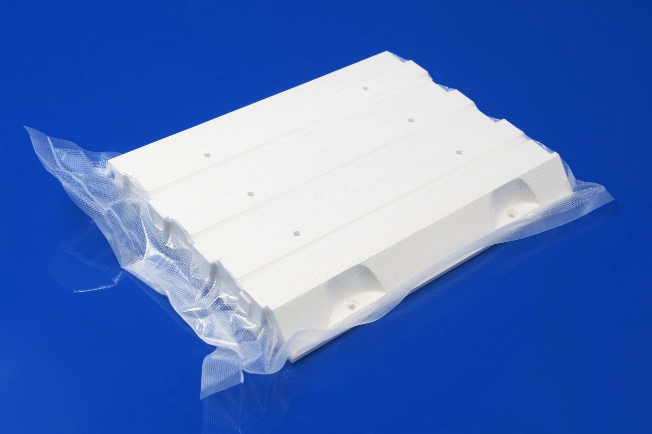
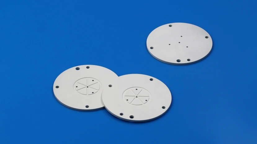
Typical applications include electrical isolators, high-temperature furnace fixtures and components used in vacuum or inert-atmosphere processes. BN grade selection should consider purity, dielectric requirements, mechanical strength, thermal performance, process atmosphere and contamination-control requirements. For plasma-facing locations, gas chemistry, ion energy and contamination limits should be reviewed before selecting a BN grade. Maximum service temperature and vacuum suitability also depend on grade composition and atmosphere.
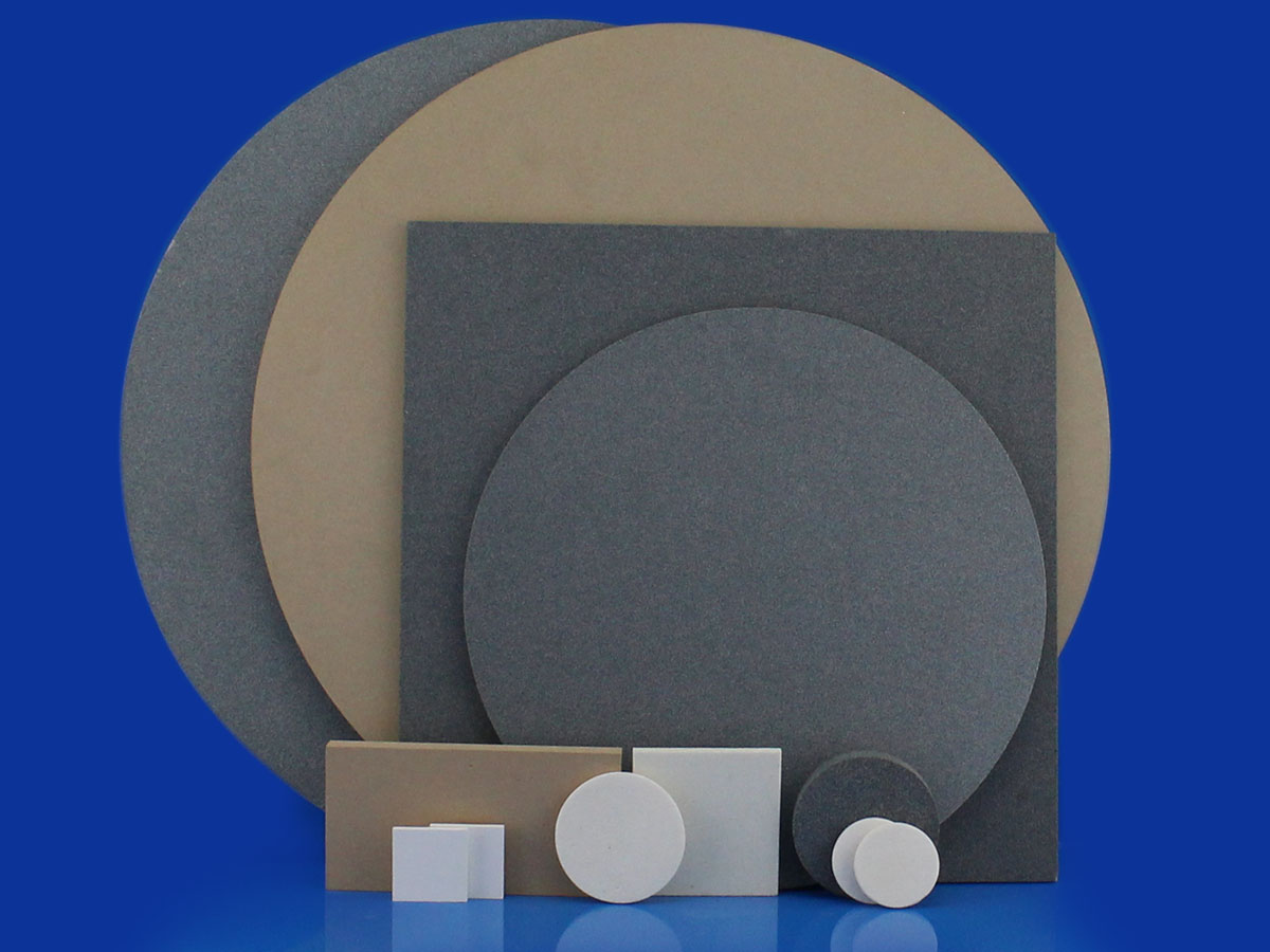
2. Ceramic Wafer Chucks and Wafer-Support Components
Wafer-support components are used in handling, inspection, LED processing, etching, deposition and other semiconductor operations. The holding method and ceramic architecture depend on whether the tool operates at atmospheric pressure, under vacuum or inside a process chamber.
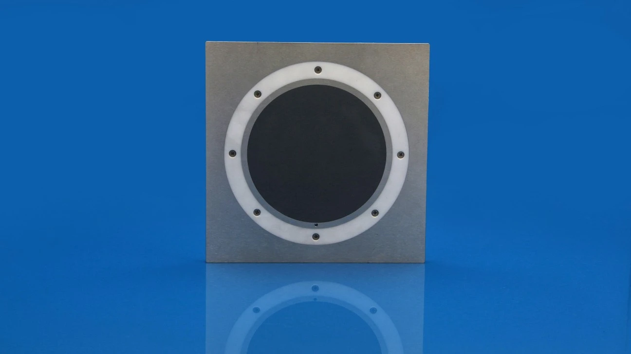
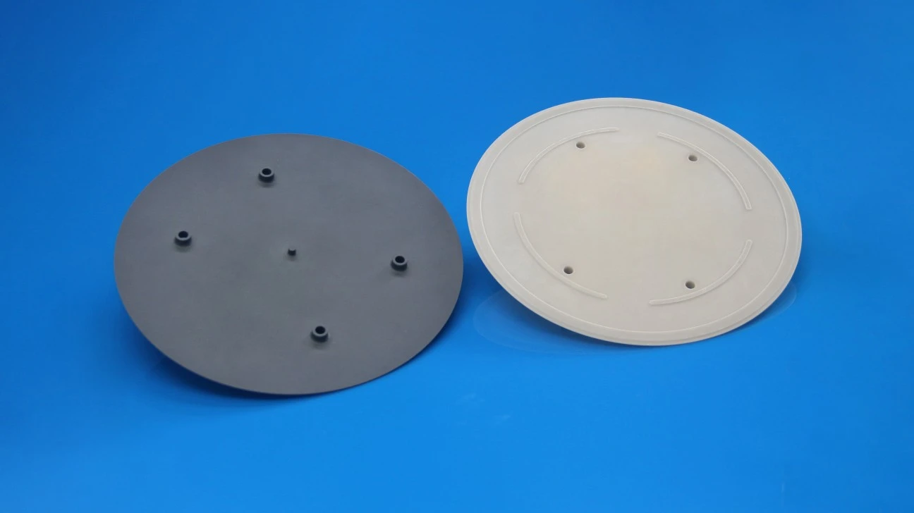
Vacuum chucks use a pressure differential and are common in handling and inspection applications. Inside vacuum process chambers, ceramic parts may instead form part of electrostatic, heated or temperature-controlled chuck assemblies, depending on the equipment design.
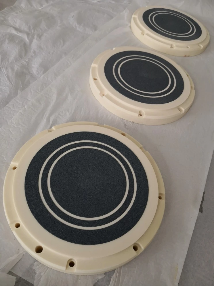
Key design inputs include wafer size, flatness, surface roughness, contact geometry, vacuum-hole or pore distribution, groove layout, mounting features, operating temperature and backside-contact requirements.
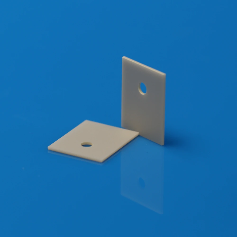
3. Alumina Rings And Plates
Alumina is a practical main choice for semiconductor processing that need electrical insulation, wear resistance, mechanical stability and mature precision-machining capability. Common forms include rings, plates, bases, insulators, supports and custom machine parts.
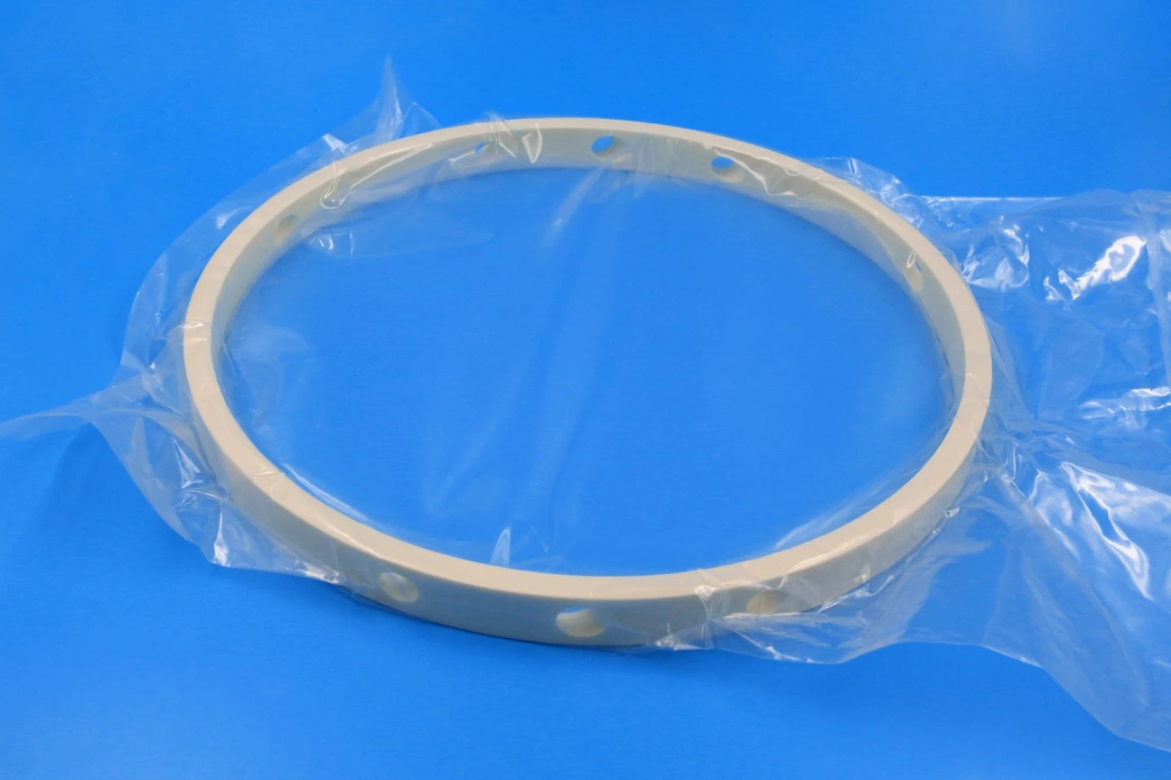
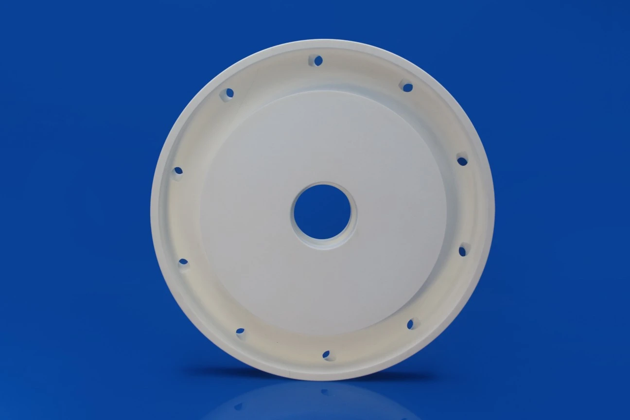
For large or thin components, post-sinter machining is critical. Flatness, parallelism, hole position, edge geometry and surface finish should be defined on the drawing and verified against the assembly requirement.
For plasma-facing chamber parts, purity, trace-element control and plasma-erosion behavior should be evaluated separately. A semiconductor-grade or plasma-optimized alumina grade may be required depending on process chemistry.
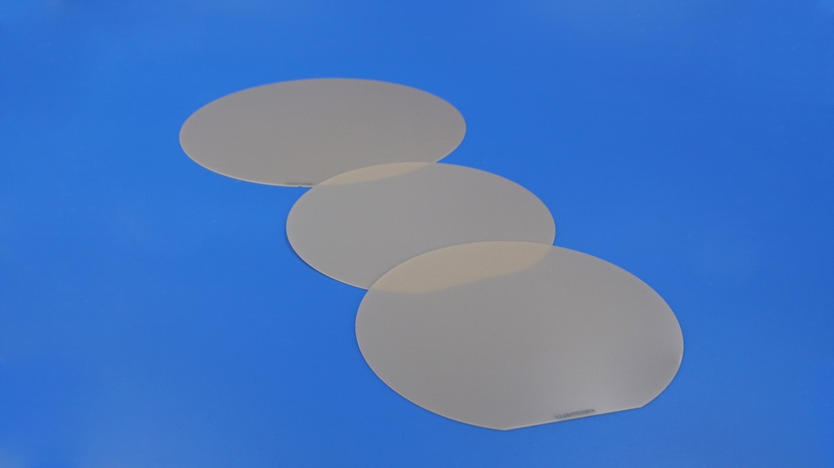
4. Aluminum Nitride Wafers for Thermal Management and Wafer Support
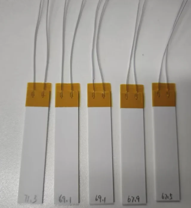
Aluminum nitride is used when electrical insulation must be combined with significantly higher thermal conductivity than conventional alumina. Typical functions include heated or temperature-controlled platforms, thermal spreaders, electrically insulating heat-transfer structures and wafer-support components.
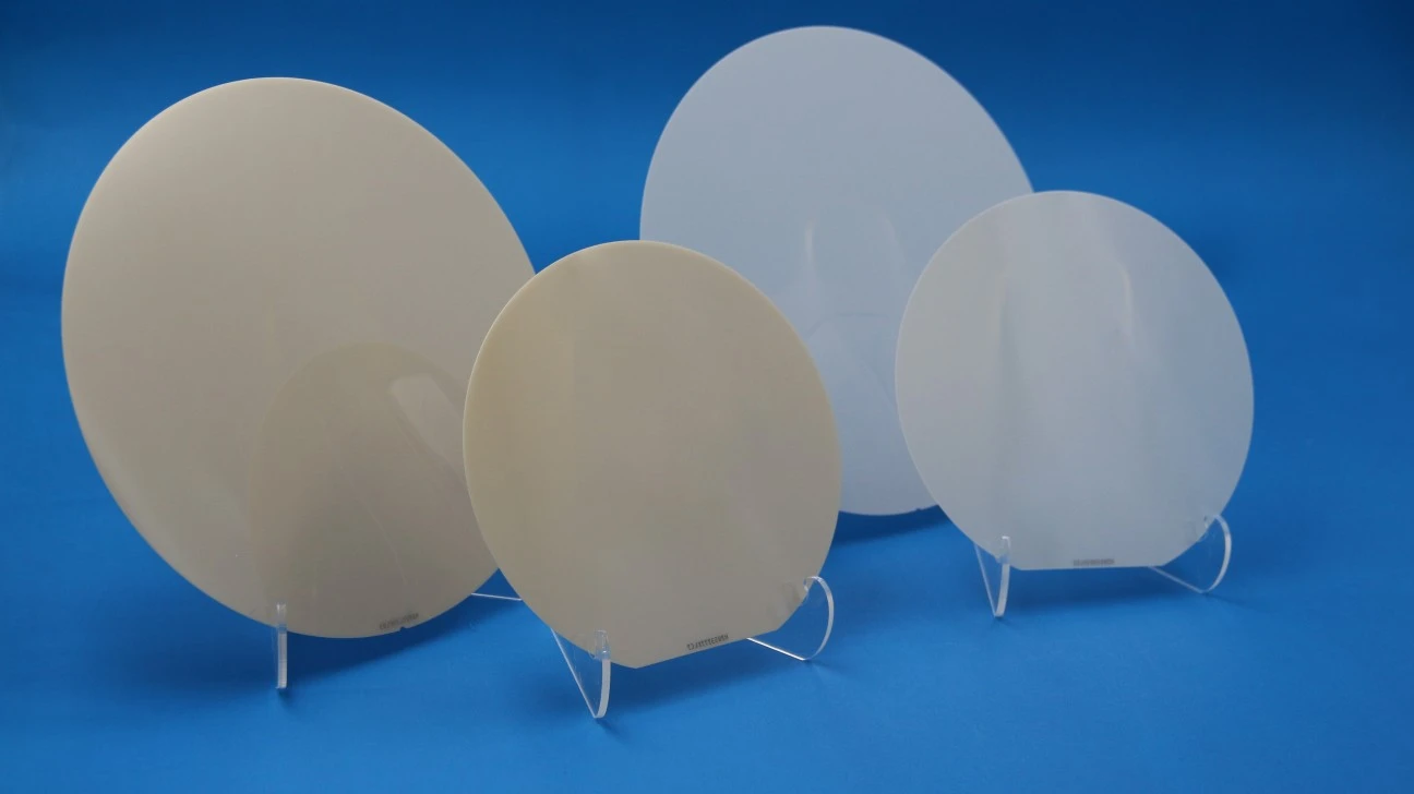
These AlN wafers are precision-machined polycrystalline technical-ceramic components rather than single-crystal semiconductor substrates. They can be ground and machined with mounting holes, gas passages, grooves and other functional features.
Material selection should consider thermal conductivity together with operating temperature, plasma chemistry, electrical requirements, mechanical loading, surface condition and cost.
5. Ceramic Arms and Wafer-Handling End Effectors
Wafer-transfer systems require high specific stiffness, dimensional stability and controlled geometry for repeatable positioning. Alumina ceramic arms and end effectors can also provide electrical insulation and wear resistance where these properties are required by the tool design.
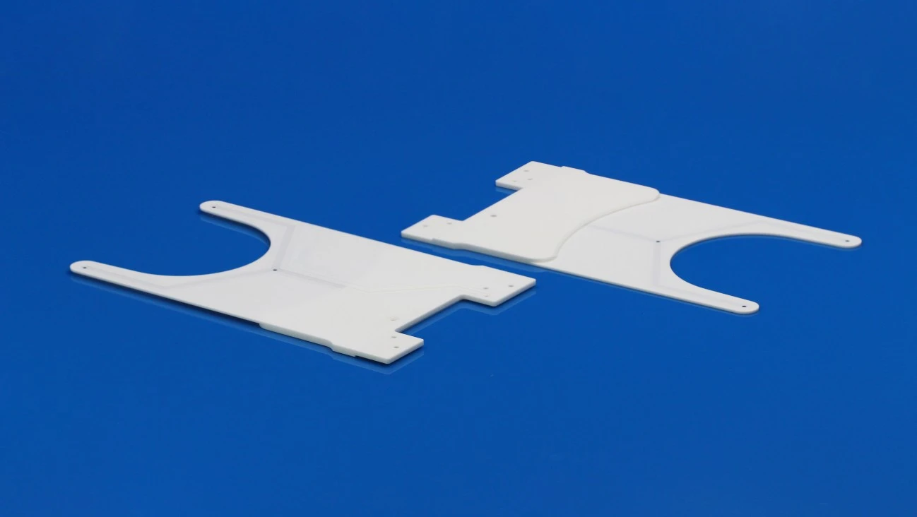
The final geometry should be checked against wafer size, payload, acceleration, mounting stiffness, robot kinematics and the process environment.
6. Ceramic Bonding Tools for Semiconductor Packaging
Ceramic bonding tools are used in wire-bonding and related packaging processes where wear resistance, geometry stability and precise working features are required.
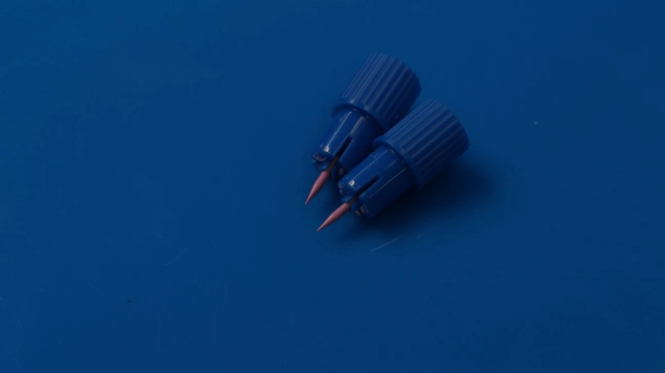
Important variables include tip geometry, small-hole dimensions, surface condition, wire material and batch-to-batch consistency. Tool geometry and ceramic grade should be matched to the bonding process and equipment configuration.
7. Material Selection Guide
No single ceramic is best for every semiconductor application. Select the material against the dominant engineering requirement and the process environment.
| Material | Primary Engineering Value | Key Design Check | Typical Uses |
|---|---|---|---|
| BN | Electrical insulation, machinability, high-temperature use | Grade, atmosphere, strength, plasma/contamination limits | Insulators, electrode-adjacent parts, high-temperature supports, complex machined parts |
| Al₂O₃ | Electrical insulation, wear resistance, structural stability | Purity, plasma chemistry, flatness and machining tolerance | Rings, plates, chucks, insulators, robot arms, structural parts |
| AlN | High thermal conductivity plus electrical insulation | Thermal load, plasma chemistry, machining and cost | AlN wafers, heated platforms, chuck components, thermal-management parts |
| SiC | High stiffness, hardness, wear resistance, useful thermal performance | Dense vs porous grade, electrical behavior, surface architecture | Porous vacuum surfaces, wear parts, high-stiffness supports |
8. Information Required for a Custom Ceramic Part
For engineering review, provide the information that controls material choice and manufacturability:
- 2D/3D drawing, critical dimensions and tolerances
- Flatness, parallelism and surface-roughness requirements
- Wafer size, contact method and holding method
- Operating temperature and thermal-gradient requirement
- Vacuum level, gas chemistry or plasma environment
- Electrical-insulation, thermal or wear requirement
- Cleaning, inspection and expected quantity requirements
| INNOVACERA supplies custom BN, alumina, AlN, SiC and other advanced ceramic components for Semiconductor Industry. Send the drawing and operating conditions for material and manufacturability review. |
|---|