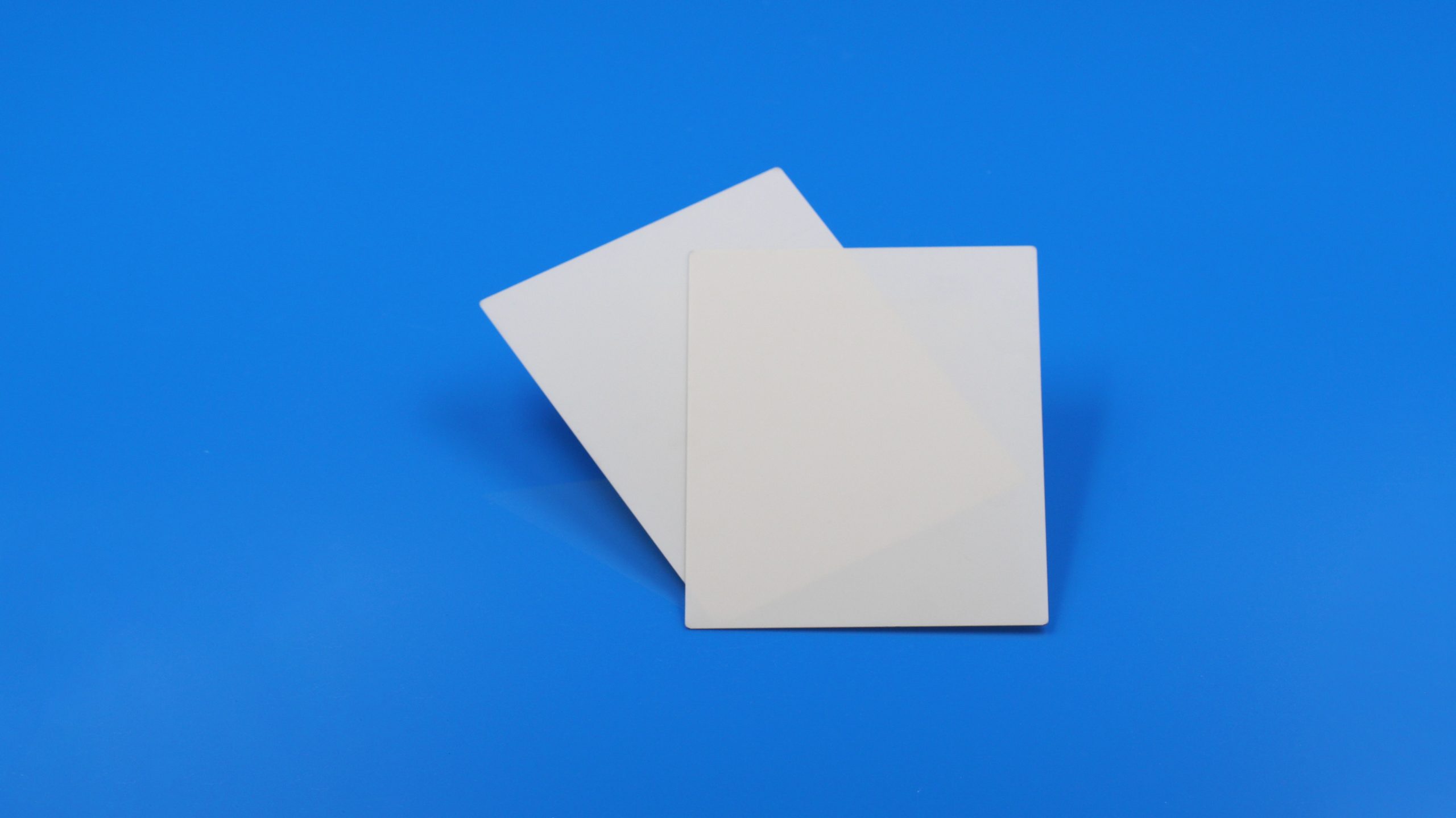
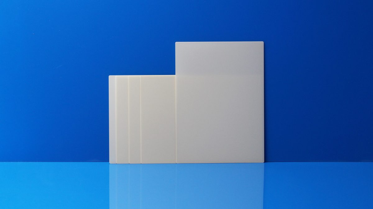
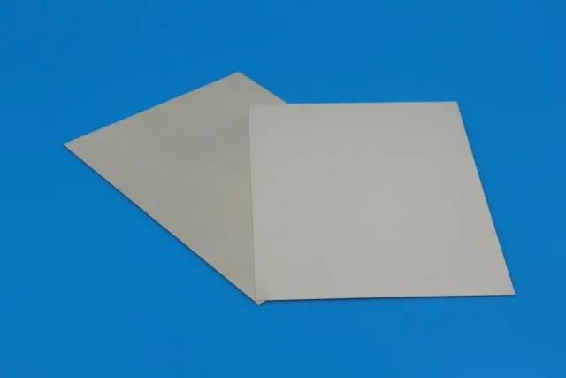
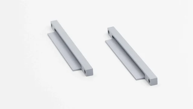
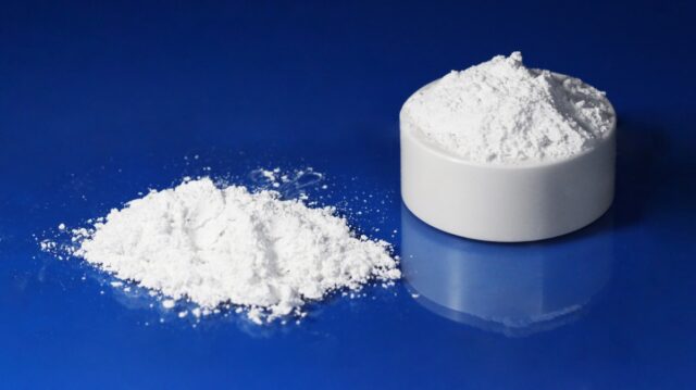
Ceramic substrates show up with all kinds of surface finishes, and the one you pick can steer your whole process in a good direction—or a frustrating one. If you’ve ever sat with a spec sheet wondering which option actually makes sense, you’re not the first.
Each finish solves a different problem. Pick the wrong one and you’re either overpaying or chasing defects. Here’s what they each actually do, stripped of the marketing speak.
As-Fired: Straight Out of the Oven
This one’s simple. The substrate gets sintered, it cools, and that’s it—no extra work on the surface. What you see is what the firing process left behind.
Appearance: Matte and slightly rough, with a fine grain texture. On alumina, Ra typically measures 0.3–0.6 μm.
Where it fits: Jobs that don’t demand much from the surface. Thick-film printing, basic resistor networks, heating elements, and structural parts all do well here. The main advantage is efficiency—you skip entire processing steps and keep production moving.
What to watch: The dimensional control isn’t tight. Thickness can wander, and flatness isn’t guaranteed. If your process needs accurate alignment, as-fired will test your patience.
Lapped: Flatter, Period
Lapping takes the substrate and runs it across a rotating plate with abrasive slurry. It grinds down the high spots and gets the whole thing more uniform.
Appearance: Still matte, but visibly smoother and more consistent than as-fired. Ra lands in the 0.1–0.4 μm range.
Where it fits: This is the utility player. You get better flatness without going all the way to a polish. Most thin-film processes run fine here. The improved evenness also tightens up registration from part to part.
What to watch: This route takes more work and more time. And if the lapping is too aggressive, you can introduce tiny subsurface cracks. That said, for most commercial work, the benefits outweigh those concerns.
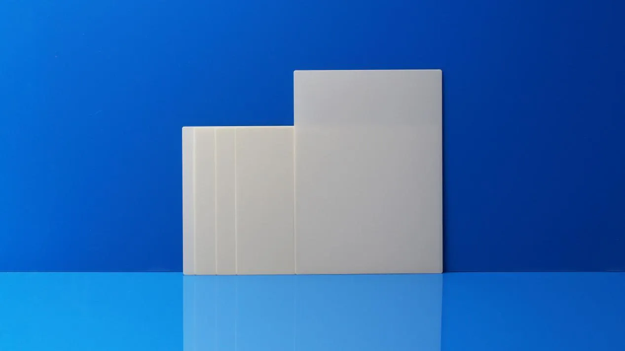
Polished: Glass-Level Smooth
Polishing takes lapping further. Progressively finer abrasives work the surface until it reflects light like a mirror.
Appearance: Shiny and smooth. Standard grades hit Ra ≤ 0.1 μm; special grades go down to ≤ 0.05 μm.
Where it fits: High-end thin-film work—dense circuitry, fine-line lithography, optical uses, or any situation where surface flaws are non-negotiable. Also when the substrate needs to mate flush with another surface.
What to watch: This is the most demanding route. More operations, more handling, more opportunities for scrap. Spec it when you genuinely need it, but don’t assume it’s better just because it’s more elaborate.
Quick Look
| Finish | Ra Range | Suited For |
|---|---|---|
| As-Fired | 0.3–0.6 μm | Thick-film, low-cost basics |
| Lapped | 0.1–0.4 μm | Thin-film, general use |
| Polished | ≤ 0.1 μm (≤ 0.05 μm special) | High-density thin-film, optics |
How to Choose
Think about three things:
1. What’s your line width? Bigger features get by with as-fired. When the pitches tighten, lapped or polished becomes necessary.
2. What’s your production volume? Higher volumes may justify the extra processing for better consistency. Lower volumes might not.
3. What comes next in your line? Thin-film deposition likes smooth. Thick-film paste actually prints better when there’s a little tooth to grab onto. Let your process decide for you.
Most suppliers stock all three and can show you samples. Sometimes just feeling the difference in your hands beats reading numbers off a page.