technical ceramic solutions

Laser Cutting and Singulation Techniques for AlN Ceramic Substrates in Advanced Semiconductor Packaging

Publish Date: by Innovacera

When developing power semiconductors and advanced semiconductor packaging, effective thermal management has become a critical challenge, and aluminum nitride (AlN) substrates have emerged as a primary material to solve heat dissipation issues. However, machining these rigid, fragile ceramic boards has long been a major pain point. Traditional mechanical dicing methods show obvious limitations: they easily cause edge chipping and microcracks, while frequent tool replacement also raises overall production costs.


Laser cutting and singulation techniques provide a practical alternative for 138×190 mm AlN mother panels, commonly available in 0.5 mm and 0.635 mm thicknesses. Many manufacturers now adopt ultraviolet (UV) lasers and picosecond ultrafast lasers for this process, achieving consistent dimensional accuracy within ±10 µm. The ultrafast laser processing creates an extremely narrow heat-affected zone, greatly reducing thermal damage and residual microcracks in the ceramic substrate.
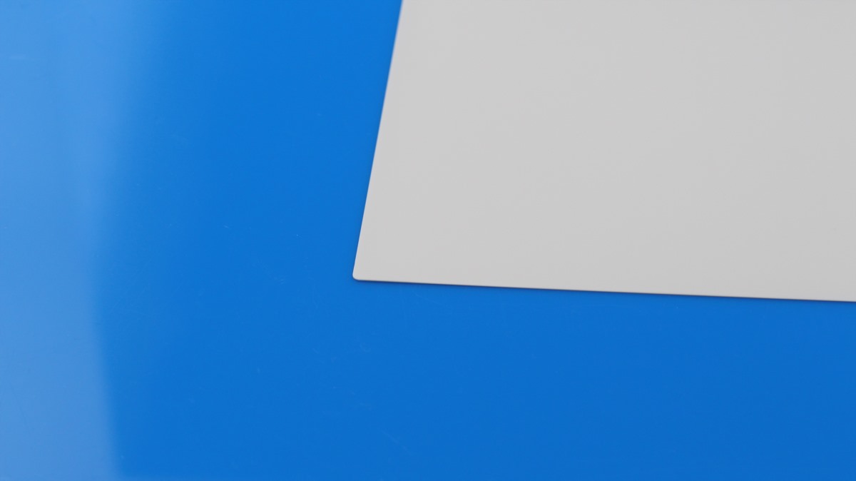
 

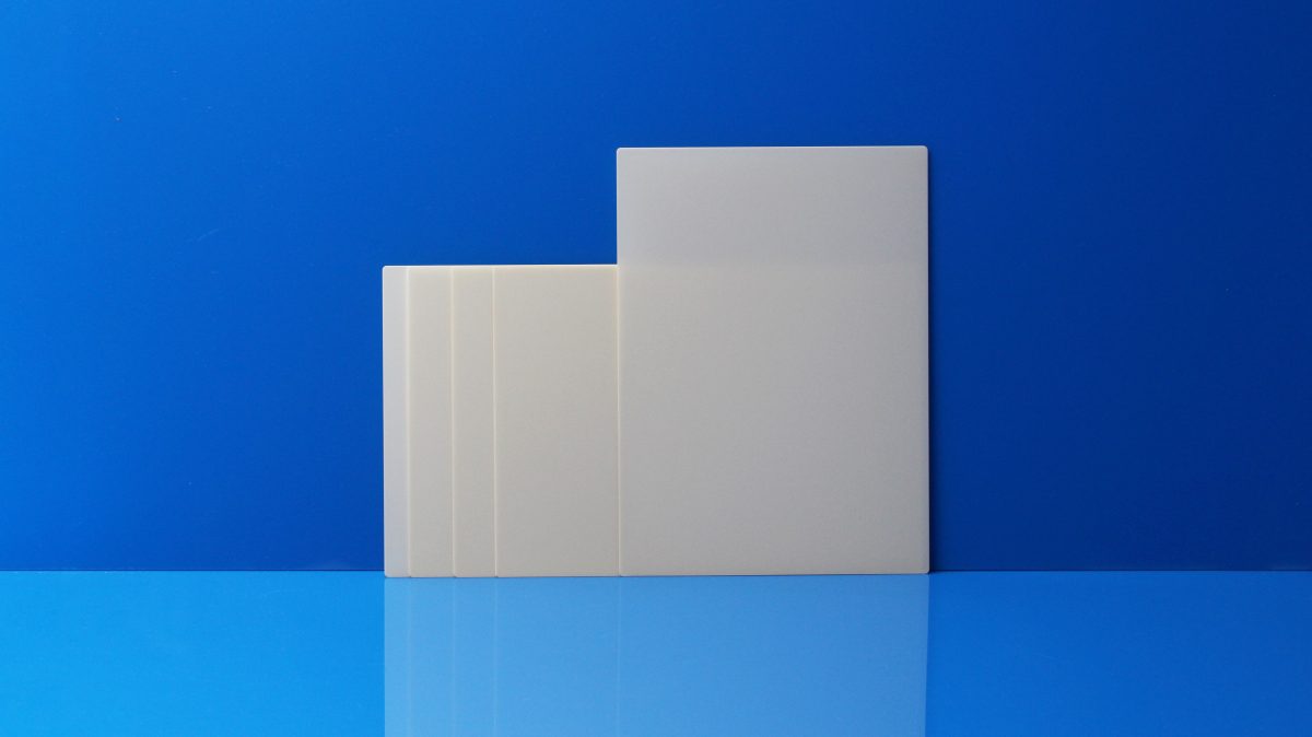
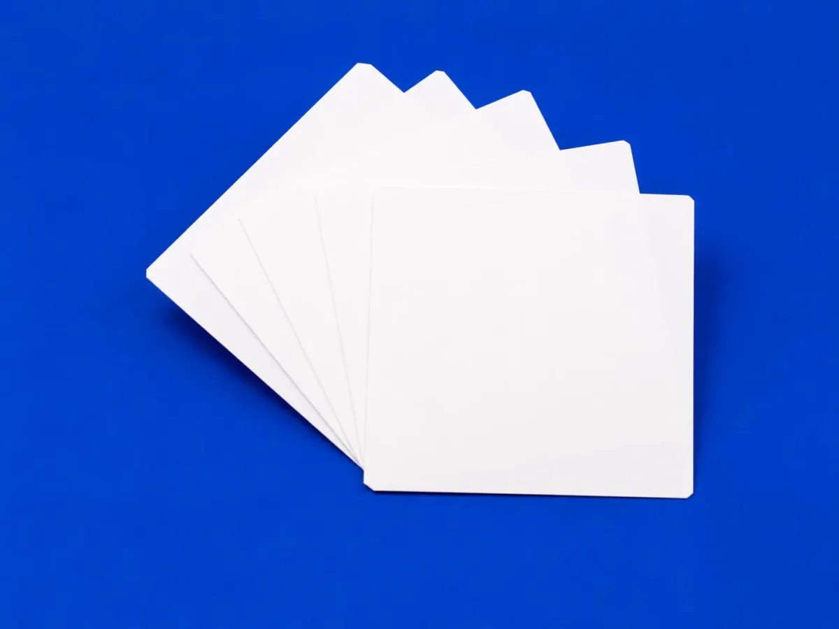
Aluminum_Nitride_Master_Sheets


For 0.635 mm thick AlN sheets, high-power picosecond lasers can reach a cutting speed of roughly 300 mm/min for the 138×190 mm panel format. The scribe-and-break process, which only performs partial laser scribing rather than full through-cutting, further increases production throughput by 50%, bringing clear efficiency improvements to mass production lines.


There remain key practical hurdles for large-format AlN panels. Thin, big substrates are prone to warpage and uneven flatness across the surface, which can shift the laser focal position during processing. Even minor focal drift will lead to inconsistent cutting quality and reduce final singulation yield. Therefore, proper substrate fixturing and flatness control are just as essential as optimizing laser process parameters.
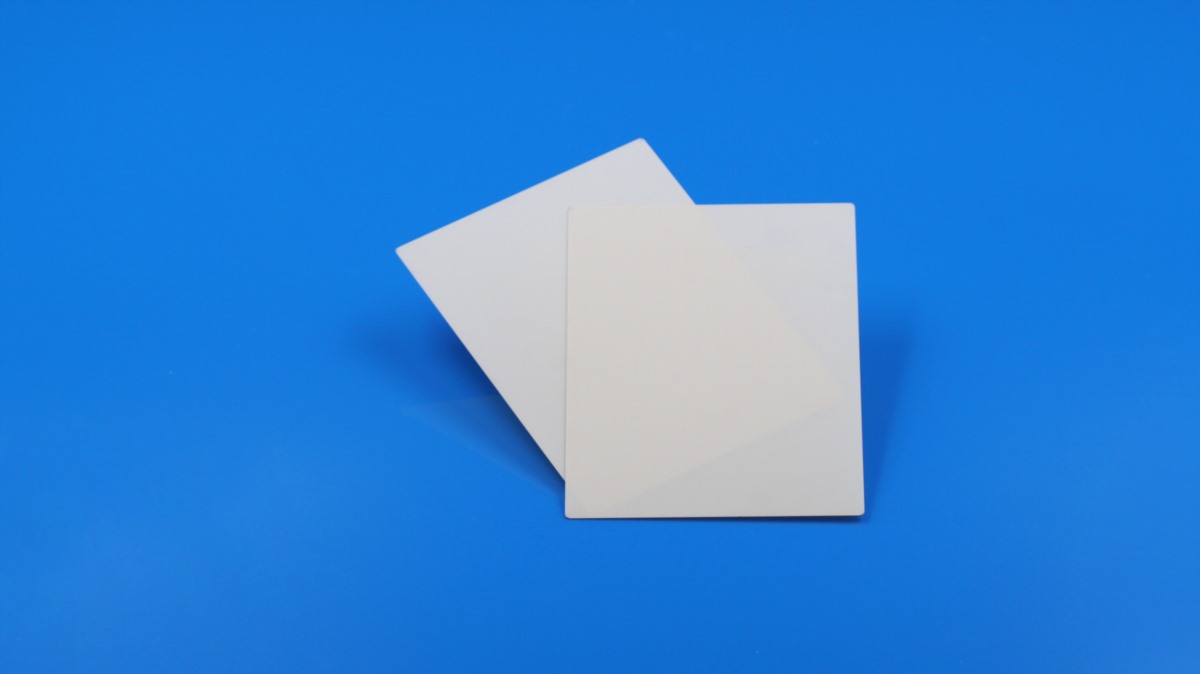
 

Laser Cutting and Singulation of 138 × 190 mm Aluminum Nitride Master Sheets


Overall, ongoing improvements in laser reliability and cost-effectiveness are gradually eliminating AlN panel singulation as a key production bottleneck. A growing number of electronics manufacturers are transitioning to laser-based processing, with real-world production data confirming its advantages.
Declaration: This is an original article of INNOVACERA®. Please indicate the source link when reprinting: https://www.innovacera.com/news/laser-cutting-and-singulation-techniques-for-aln-ceramic-substrates-in-advanced-semiconductor-packaging.html.

FAQ

Laser singulation for AlN substrates is a precision cutting process that uses UV or picosecond ultrafast lasers to dice aluminum nitride ceramic panels into individual components. It is replacing traditional mechanical dicing because conventional methods cause edge chipping, microcracks, and high tooling costs. Laser-based processing achieves dimensional accuracy within ±10 µm, minimizes the heat-affected zone, and reduces thermal damage—making it the preferred solution for high-volume power semiconductor and advanced packaging production lines.

The scribe-and-break process is a laser singulation technique that performs only partial laser scribing on the AlN substrate rather than full through-cutting, followed by a mechanical breaking step to complete the separation. For 138×190 mm AlN mother panels, this approach increases production throughput by approximately 50% compared to full laser cutting. By reducing the total laser processing time per panel, it delivers significant efficiency improvements for mass production lines while still maintaining consistent cut quality and minimizing substrate damage.

Related Products

  • Silicon Nitride (Si₃N₄) Substrates

    Silicon Nitride (Si₃N₄) Substrates

    Innovacera's Silicon Nitride (Si₃N₄) Substrates combine exceptional thermal conductivity, high mechanical strength, and excellent fracture toughness, providing outstanding reliability for high-power e…

  • Aluminum nitride (AlN) Substrates

    Aluminum nitride (AlN) Substrates

    Innovacera’s Aluminum Nitride (AlN) Substrates deliver exceptional thermal conductivity, a thermal expansion coefficient closely matched to silicon, and excellent electrical insulation, making them an…

  • 96 Alumina (Al₂O₃) Substrates

    96 Alumina (Al2O3) Substrates

    Innovacera’s 96 Alumina (Al₂O₃) Substrates combine high density, superior thermal conductivity, and excellent dielectric strength, making them an ideal choice for electronic and energy applications. W…

Enquiry