Yesterday was special for us: Innovacera was celebrating 7th birthday on August 8th, 2019.
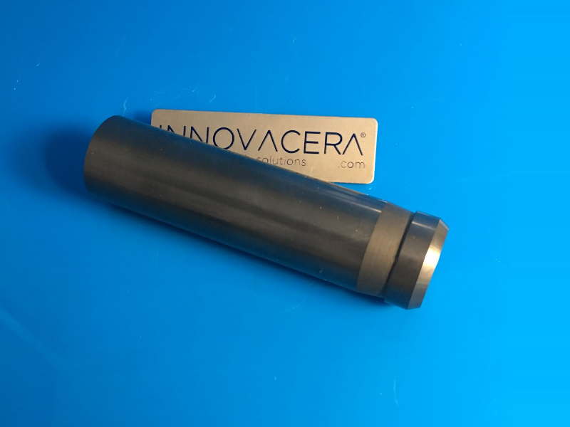
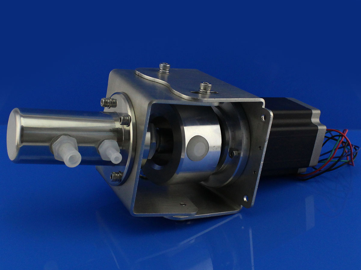
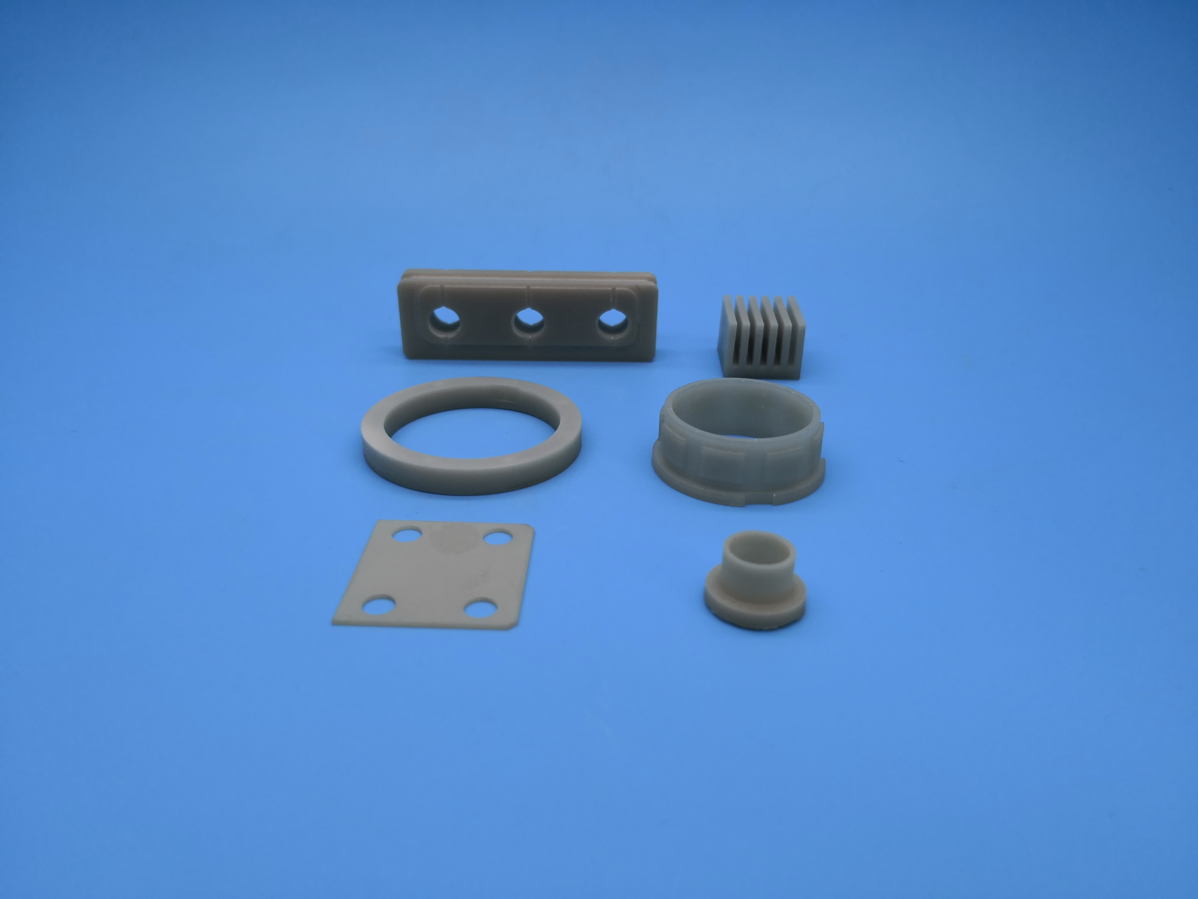
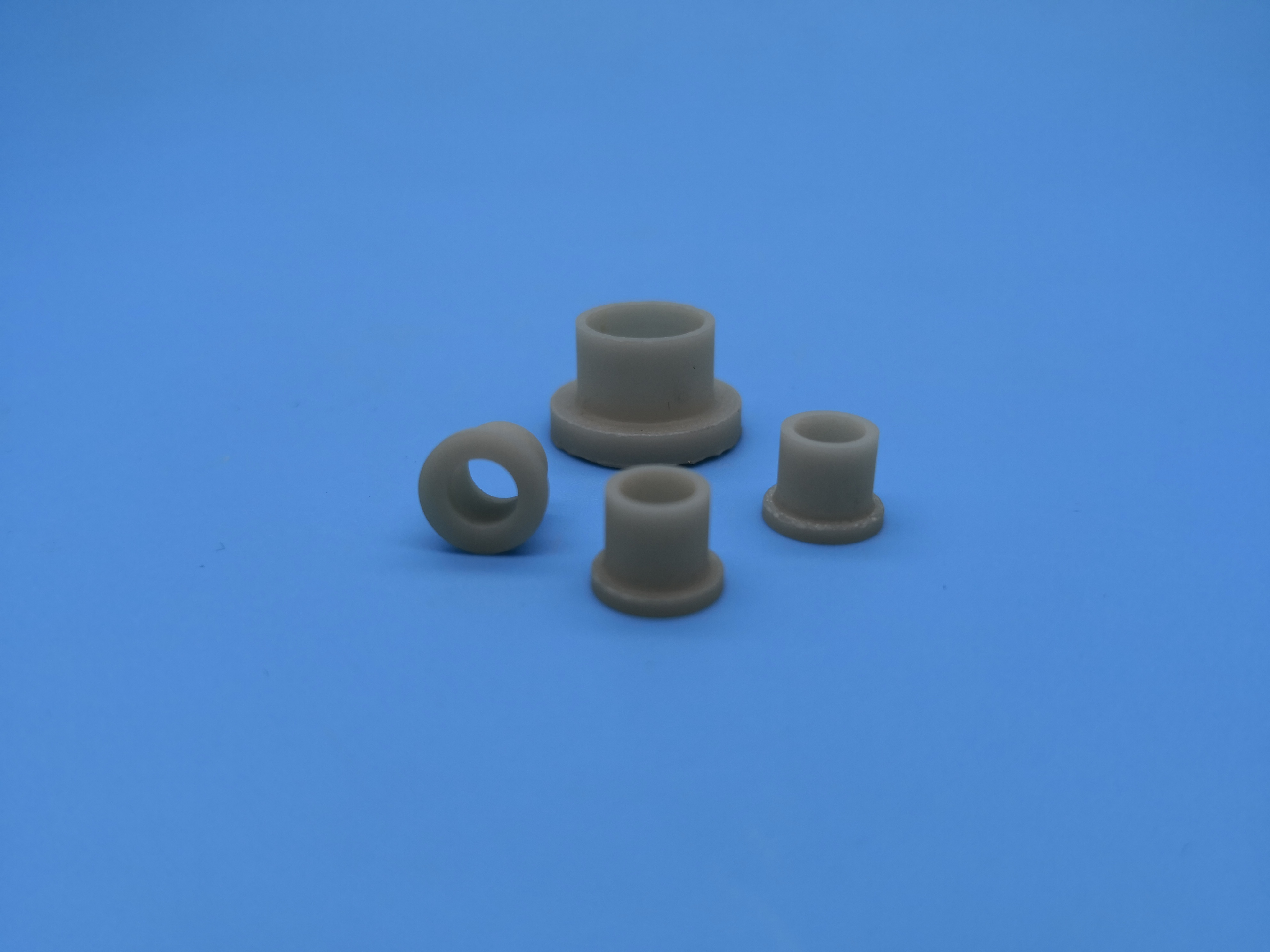
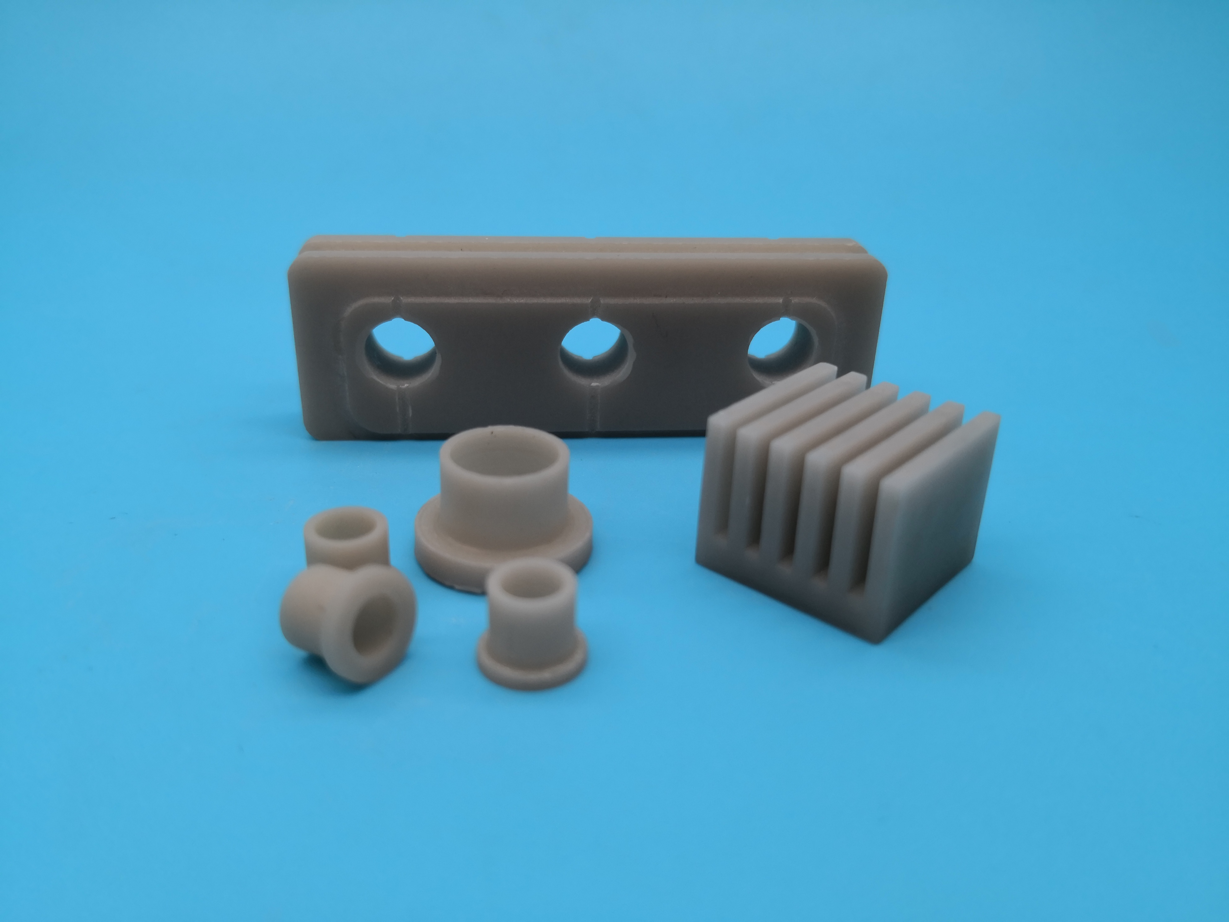
On 8 August 2012, Innovacera established for providing the ideal technical ceramic solution for many industries. Innovacera has two factories which are responsible for manufacture. Our engineer is with experience in R&D, manufacture and sales in advanced ceramic materials for more than 20 years. The sales office(Innovacera) was established 7 years ago, serving international clients, today is a recognized reliable technical ceramic supplier company.
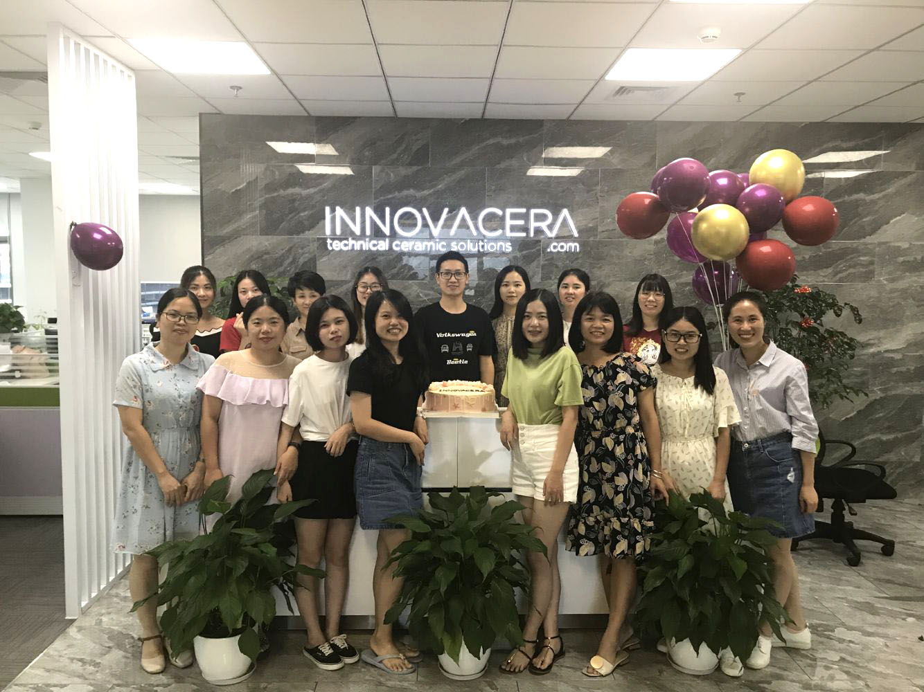
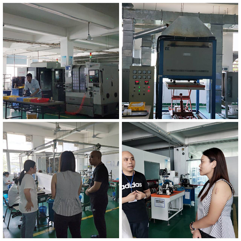
We are proud of our active team and 2 factories who are full of creativity, responsibility, professional drive, innovative ideas. We truly appreciate our team, especially grateful to those colleagues whose professional activity at Innovacera lasts over 5 years.
We would like to thank all our team who continue to work as One and put their best effort in making Innovacera as a reliable and trusted technical ceramic supplier company.
Our success depends on clients’ success. Thus, we hope that our professional knowledge contribute to our clients’ success and to building sustainable society as well. We are positive that when our clients are stronger, so are we.
At this 7th anniversary, we would like to take this opportunity to thank all our clients for including Innovacera in their business story for the past 7 years. We look forward to successful cooperation in the future!
We will keep to work closely with clients to help provide the qualified ceramic products to meet unique and demanding performance requirement in further 10, 15, 20, 25…years and never stop.
 Enquiry