.svg)
In the pursuit of high performance and high reliability in electronic manufacturing, traditional substrate materials have become increasingly unable to meet the ever more demanding requirements. Limited thermal conductivity, poor high-temperature stability and insufficient surface accuracy are becoming the bottlenecks for the development of thick-film and thin-film circuits. Therefore, the industry urgently needs a new type of carrier that combines excellent insulation, efficient heat dissipation, outstanding dimensional stability and ideal surface flatness to support the printing and sintering processes of precision circuits.
Core performance requirements of thick film/film circuits for the substrate:
In the field of high-performance electronics, thick-film and thin-film circuits are two crucial microfabrication technologies. Although their processing paths are different, they both impose many similar and stringent requirements on the substrate materials that carry their circuits.
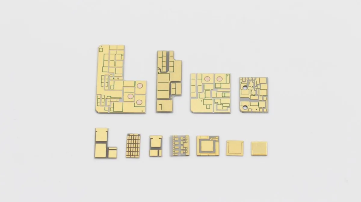
The thick-film circuit is formed by applying conductive, resistive or insulating pastes through screen printing on the surface of the substrate, and then undergoing high-temperature sintering for solidification to create the circuit pattern. The typical sintering temperature is approximately 850℃ – 900℃, and the specific temperature depends on the type of slurry and the substrate. The core of its process requires that the substrate must be able to withstand high-temperature thermal shock, maintain extremely high dimensional stability (without warping or shrinking) and chemical inertness during the sintering process, prevent reactions with the paste, and at the same time, the surface must meet the required flatness and adhesion for printing.
The thin-film circuit adopts processes such as vacuum coating, lithography and etching to fabricate fine lines at the micrometer or even nanometer scale on the substrate. This requires that the surface of the substrate have an extremely low roughness (almost atomic-level smoothness) to ensure the precise formation of the circuits, and it must have excellent uniformity of microstructure and chemical purity to prevent the introduction of defects or impurities during the manufacturing process.
Overall, although the implementation methods of the two technologies are different, they both require that the substrate material must possess excellent thermal stability, precise surface characteristics, outstanding dimensional integrity, and stable chemical properties. Traditional organic or metal substrates often fall short in such high-end applications. However, ceramic substrates are the ideal material designed to address these demanding challenges. Their unique performance combination perfectly meets the ultimate requirements of thick film and thin film circuits for the base carrier.
The advantages of ceramic substrates directly address the pain points of high-end circuits
(1) Ultimate thermal stability and dimensional rigidity
Ceramic materials (such as Al₂O₃ and AlN) possess high melting points and excellent thermal stability, which ensures that they do not soften, deform or shrink at the thick film sintering temperature. This “rigidity” ensures precise alignment of multi-layer circuits, reduces internal stress during sintering, and enhances long-term reliability. The thermal expansion coefficients of different materials can be matched with semiconductors or printing pastes, further reducing thermal stress.
(2) Surface and Precision Machinability
For thin-film circuits, the ceramic substrate can be precisely polished to achieve a nanometer-level flatness (Ra), ensuring the accuracy of photolithography and coating processes.; For thick-film circuits, a moderately rough surface can enhance the adhesion of the paste. The ceramic substrate can be flexibly adapted to different process requirements through surface treatment.
(3) Excellent chemical purity and inertness
Advanced ceramic raw materials have high purity, dense structure, and strong chemical stability under high temperatures or in a vacuum environment. During thick film sintering, it will not react with Ag/Ag-Pd and other pastes; In the film manufacturing process, reducing low-volatile impurities can minimize vacuum contamination and defects, thereby increasing the yield of the finished products.
(4) Outstanding thermal management capabilities
High thermal conductivity (AlN can reach 150–200 W/m·K) enables the heat generated by power devices to diffuse rapidly, preventing local overheating and enhancing the reliability and thermal stability of the devices.
(5) Mechanical strength and long-term reliability
The high hardness and high bending strength ensure that the ceramic substrate is unlikely to break during processing, transportation and long-term use; the temperature cycling resistance, moisture heat resistance and corrosion resistance make the ceramic substrate suitable for high-reliability scenarios such as automotive, aviation and industrial control.
Overall, the comprehensive advantages of ceramic substrates in terms of heat, mechanical, chemical and surface properties make them an ideal platform for supporting thick film and thin film precision circuits, and also meet the requirements of high power, high density and high precision in electronic design.
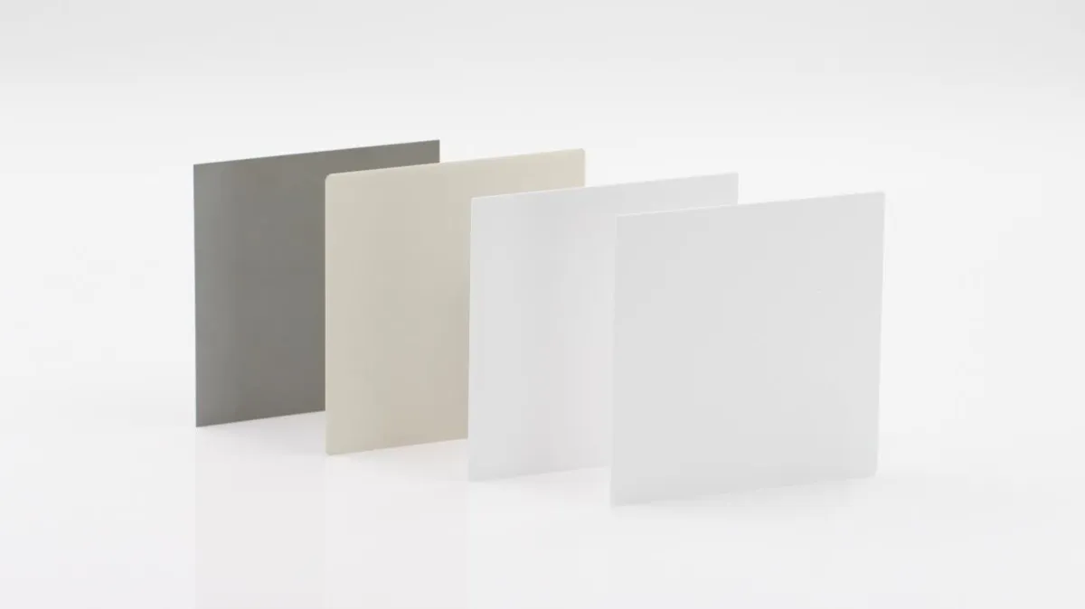
Innovacera offers a variety of ceramic substrate materials to support customers’ diverse applications in thick- and thin-film circuit printing. For inquiries, please feel free to contact us.
Declaration: This is an original article of INNOVACERA®. Please indicate the source link when reprinting: https://www.innovacera.com/news/pain-points-in-thick-and-thin-film-circuit-fabrication-and-ceramic-substrate-advantages.html.
 Substrates")


 Enquiry