The molecular beam epitaxy ( MBE Crucible ) method is one of the methods to produce gallium arsenide epitaxy wafers. This method can be used to produce multiple, multilayer, homogenous, heterogenous, superlattice, and quantum well epitaxy materials. High crystal purity and good chemical stability. MBE Crucible is mainly used to synthesize semiconductor single crystal and ⅲ-ⅴ group compounds by MBE method.
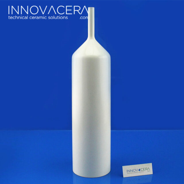
Pyrolytic Boron NitridePBN Ceramic MBE Crucible for Microelectronics Industrial
MBE Crucible Main Features
1. Can make large crucible (maximum diameter 12inch, maximum height 17inch);
2. High density (up to 2.2g/cm3);
3. High purity (>99.99%);
4. Not easy to crack (high interlayer strength).
PBN Properties
| Technical Parameter | BN | PBN | ||
|
Mechanical |
Density | g/cm3 | 2.2~2.3 | 2.1-2.19 |
| Color | — | White | White | |
| Water Absorption | % | 0 | 0 | |
| Vickers Hardness | Gpa | (Moh’s=2) | (Knoop=691) | |
| Flexural Strength (20°C) | Mpa | 100 | 243.63 | |
| Compressive Strength (20°C) | Mpa | 287 | — | |
|
Thermal |
Thermal Conductivity (20°C) | W/m.K | 35 | 43-60 |
| Thermal Shock Resistance (20°C) | Δ T(C) | — | — | |
| Maximum Use Temperature | °C | 2400 | 2200 | |
| Electrical | Volume Resistivity (25°C) | Ω.cm | 10 ^ 8~10 ^ 13 | 3.11×10 ^ 11 |
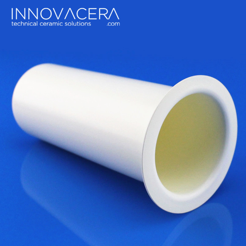
Pyrolytic Boron NitridePBN Ceramic MBE Crucible for Microelectronics Industrial (2)
Declaration: This is an original article of INNOVACERA®. Please indicate the source link when reprinting: https://www.innovacera.com/news/pyrolytic-boron-nitride-pbn-ceramic-mbe-crucible-for-microelectronics-industrial-2.html.

 Enquiry