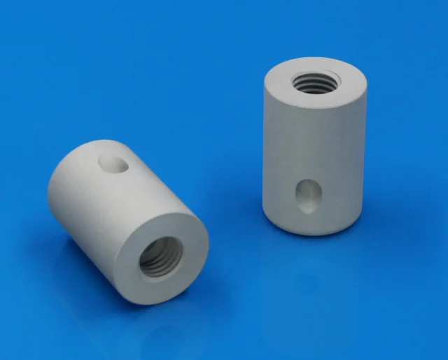
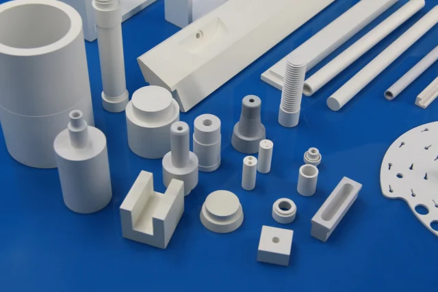
With the advancement of optical communication technology, optical modules must support high-speed optoelectronic signal conversion, electrical connections, and component mounting within increasingly compact packaging spaces, while maintaining stable long-term operation. For optical transmitter and receiver components, the installation methods of internal chips, pins, and other optoelectronic devices significantly influence subsequent packaging design.
Ceramic packages are used in the packaging of certain optoelectronic devices. They not only serve to mount and protect internal components but can also, through metallization processes, metal leads, and brazing structures, provide electrical insulation and external connectivity.
However, not all optical modules utilize ceramic packages. Whether ceramic packaging is required depends on the device structure, electrical requirements, thermal design, and packaging process.
1. What role do ceramic packages play in optical transmitter and receiver assemblies?
An optical communication module typically includes optical transmitter and receiver components. The optical transmission component converts electrical signals into optical signals and then outputs them through an optical structure; the optical reception component receives the optical signals and converts them back into electrical signals.
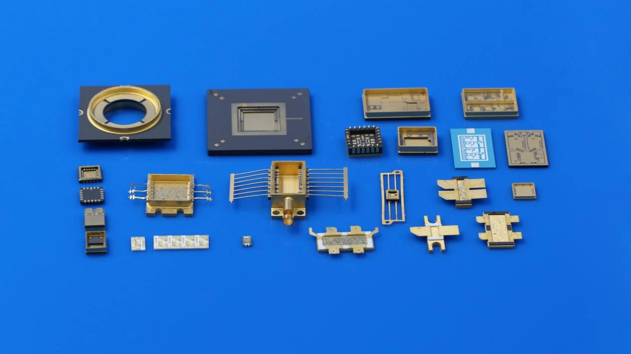
Although the tasks of these two components are different, some similar issues need to be addressed during the packaging process, such as how to fix the internal components, how to achieve electrical connections, and whether the entire structure can remain stable. Ceramic packages provide both structural support and electrical insulation for internal components. After local metallization, the ceramic surface can also form areas suitable for circuit connections, chip installation, or connection with other metal components.
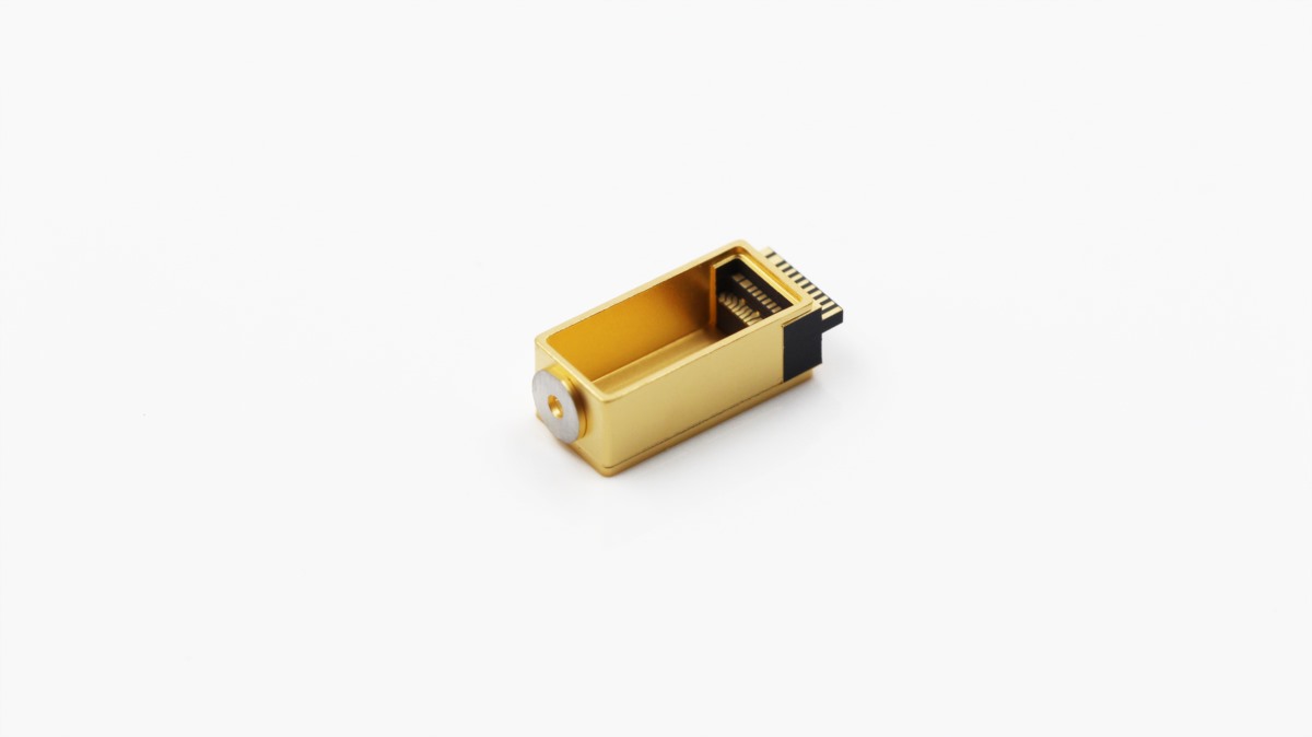
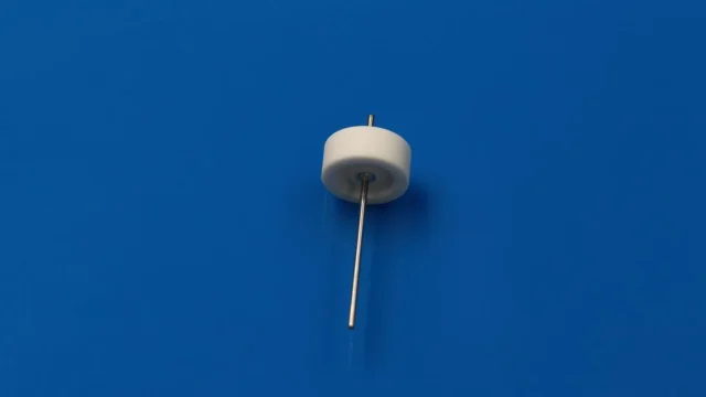
Take the ceramic package with metal pins as an example. The ceramic part is responsible for isolating different conductive areas, while the metal pins are used to connect the internal components and the external circuits. If the package requires hermetic sealing, the ceramic-to-metal joining method and the required sealing performance must also be considered during the design process.
Therefore, the ceramic package is not merely a casing for housing the chip. The selection of materials, the layout of the metallization areas, and the design of the pins and other structures all need to be determined in conjunction with the specific device.
2. Why are ceramic packages chosen for optoelectronic communication devices?
Not all optical communication devices use ceramic packages. Metal and other packaging materials are viable alternatives, selected according to device design and application needs. Engineers opt for ceramic packages mainly based on insulation specs, structural layout, and any required joints with metal parts.
One important characteristic of ceramics is their good electrical insulation. For packages with multiple pins or different conductive areas, ceramics can not only support the related components but also help to isolate different conductive parts. The performance of different ceramic materials also varies. When selecting materials, not only the insulation performance should be considered, but also the thermal expansion characteristics, dimensional accuracy, and subsequent processing requirements. These factors will all affect the assembly of the device and the connection effect between ceramics and other components.
Ceramics can also be combined with metal components through metallization. For instance, when a package housing requires metal pins, a mounting frame, or a sealed connection structure, specific areas of the ceramic can be metallized according to design requirements, followed by the completion of the connection using processes such as plating or brazing. The specific process depends on the package design and application requirements.
Of course, ceramic packaging is not the most suitable choice in every situation. Different materials have their own characteristics in terms of thermal conductivity, thermal expansion coefficient, and processing capabilities. Ultimately, the choice depends on the structure of the device and the requirements of its use.
3. What are the differences in the package design between optical transmitter components and optical receiver components?
Optical transmitter and receiver assemblies have different functions and therefore differ in their internal component configurations and packaging requirements.
The optical transmitting component typically includes a laser chip and related electrical connections and optical components. In the packaging design, attention needs to be paid to the device installation position, electrical connections, heat transfer, and optical alignment. For the structure using a ceramic package, the ceramic base, metallization areas, and pin layout need to be coordinated with the installation method of the internal components.
The optical receiver usually includes a photodetector together with related circuitry. Its package has to accommodate the device, maintain the optical path, and provide the required electrical connections and isolation.
In high-speed optical communication, the internal layout also matters. Pin count, pin arrangement, conductive paths, and package size can all affect signal routing and overall device integration.
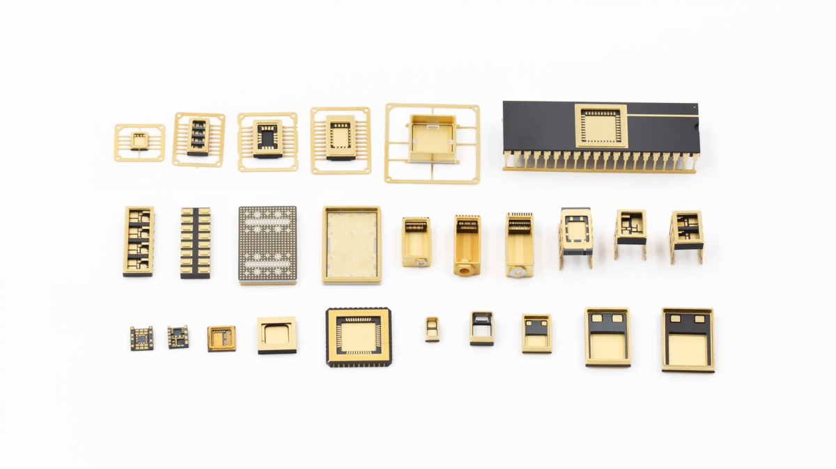
There is no single ceramic package structure that fits every transmitter or receiver design. Even when two packages look similar from the outside, their metallization patterns, pin layouts, and mounting areas can be quite different.
4. How is the electrical connection achieved for metallized ceramic packages?
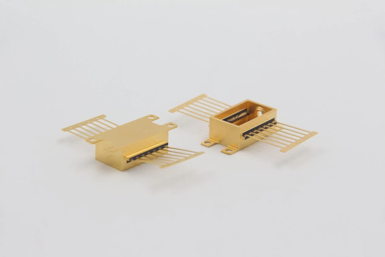
Ceramics themselves are usually insulating materials. If it is necessary to form conductive areas on the surface of ceramics or to connect ceramics with metal components, appropriate metallization and subsequent connection processes need to be adopted.
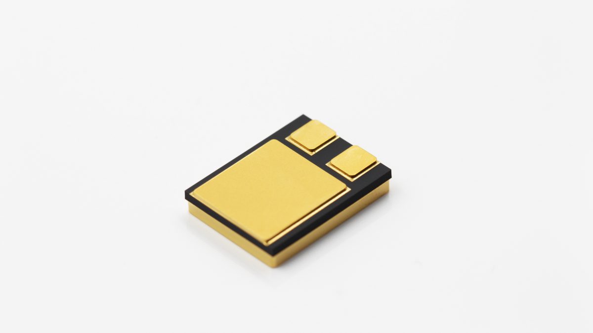
Taking certain alumina ceramic packages as an example, metallized regions can be formed at designated locations based on the product structure. These regions serve as points for electrical connections and provide a foundation for subsequent plating or ceramic-to-metal bonding.
For ceramic packages equipped with metal pins, it is also necessary to consider the method of connecting the pins to the metallized regions, as well as the insulation requirements between the various pins.
For ceramic‑metal brazed assemblies, ceramic grade, metal parts, metallization layers, brazing alloys and process parameters must be assessed as a complete system to ensure good compatibility. For hermetic optoelectronic packages, metallization and brazing alone cannot guarantee airtight integrity. Proper leak testing is required to validate sealing performance.
5. What requirements need to be confirmed when purchasing optical communication ceramic packages?
In addition to the material and overall dimensions, confirm the metallization pattern, pin layout, dimensional tolerances, and ceramic-to-metal joining requirements. For hermetic packages, confirm leak rate targets and test methods at an early project stage. Clear specifications at this stage help prevent problems during later assembly and production.
| Confirmation Item | Key Details to Confirm |
|---|---|
| Ceramic Material | Ceramic material type and corresponding performance requirements |
| Dimensions | Package outline, structural dimensions and dimensional tolerances |
| Metallization Requirements | Metallized area, pattern layout, plating layer and related process requirements |
| Leads & Electrical Connection | Number, position, pitch of leads and electrical connection method |
| Ceramic-to-Metal Joining | Whether brazing or other joining structures are required, along with corresponding joining requirements |
| Hermeticity Requirements | Hermeticity specifications, leak detection method and verification requirements |
| Assembly & Fit | Structural and tolerance requirements when mating with chips, optical components or other parts |
For custom ceramic packages, it is recommended to provide product drawings or samples when requesting a quote, while clearly specifying critical dimensions, metallized areas, pin layouts, and connection requirements. Details regarding manufacturing processes that cannot be determined immediately can be finalized later based on the specific structure and actual production requirements.
6. INNOVACERA Ceramic Packages for Optical Communication
INNOVACERA supplies metallized ceramic packages, ceramic bases, and ceramic-to-metal packages for optical communication and other optoelectronic applications. Depending on the specific requirements, designs may vary in ceramic material, overall dimensions, metallization patterns, pin arrangements, and ceramic-to-metal joining structures.
For custom projects, customers can send drawings or samples together with material requirements, key dimensions, pin details, and estimated order quantities. Our team can then review the design and confirm the manufacturing approach and supply options.
For more information, please contact sales@innovacera.com.