In the midst of the information age, as industries such as communication and microelectronics experience rapid growth, high-frequency and high-power electronic devices have become the cornerstone of the market. Ceramic materials have emerged as a favored choice for electronic device packaging due to their exceptional thermal, electrical, and mechanical stability.
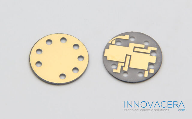
However, evolving market demands necessitate advancements in ceramic packaging technology. Central to this advancement is the critical aspect of connecting ceramics with metals. A solution is to deposit or sinter a thin metal layer on the surface of ceramics, a process commonly known as ceramic metallization. The performance of this ceramic metallization layer holds the key to determining the overall efficacy of the packaged electronic device.
Ceramic metallization layers play a crucial role in electronic device packaging for several reasons:
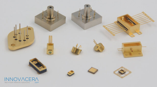
Electrical Conductivity: Ceramic materials are typically insulators, meaning they do not conduct electricity. Metallization layers are applied to ceramics to make them electrically conductive. This conductivity is vital for creating electrical connections between different components of electronic devices.
Interconnection: Electronic devices consist of various components that need to be interconnected. Metallization layers allow for the creation of conductive paths, enabling communication between different parts of the device. These paths can be highly intricate, connecting tiny components on a microscale.
Adhesion: Metallization layers can enhance the adhesion properties of ceramic substrates. Proper adhesion is necessary to ensure that the metal layer remains firmly attached to the ceramic surface, especially during the manufacturing process and the lifetime of the electronic device.
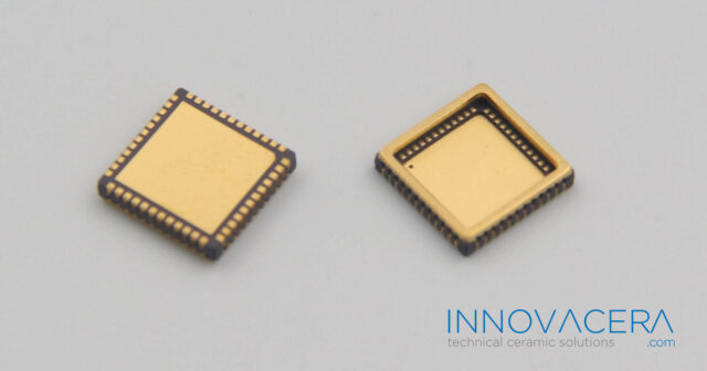
In summary, ceramic metallization layers are essential in electronic device packaging because they enable electrical conductivity, interconnection, adhesion. all of which are critical for the reliable and efficient functioning of electronic devices.
Are you seeking cutting-edge solutions for your electronic device packaging needs? Look no further! At Innovacera, we specialize in state-of-the-art ceramic metallization services. With our expertise, we ensure impeccable metallization layers that meet the highest industry standards. Our commitment to excellence guarantees the optimal performance of your electronic devices. Partner with us and experience the transformative power of superior ceramic metallization. Contact us today to explore a world where innovation meets reliability!
Declaration: This is an original article of INNOVACERA®. Please indicate the source link when reprinting: https://www.innovacera.com/news/why-is-ceramic-metallization-layer-important-in-electronic-device-packaging.html.


 Enquiry