Innovacera Adopts 50 Trees as Part of ESG Commitment at Xiamen Botanical Garden
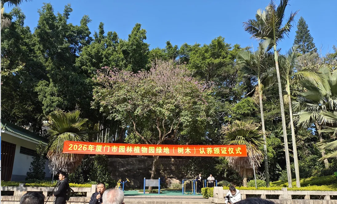
On March 12, 2026—Tree Planting Day—Innovacera employees went to the Xiamen Botanical Garden. They weren’t there just to look at flowers or trees, but to meet their “new family.” For the coming year, Innovacera will be the “foster parents” to 50 trees.
A Growing Trend of Corporate Philanthropy
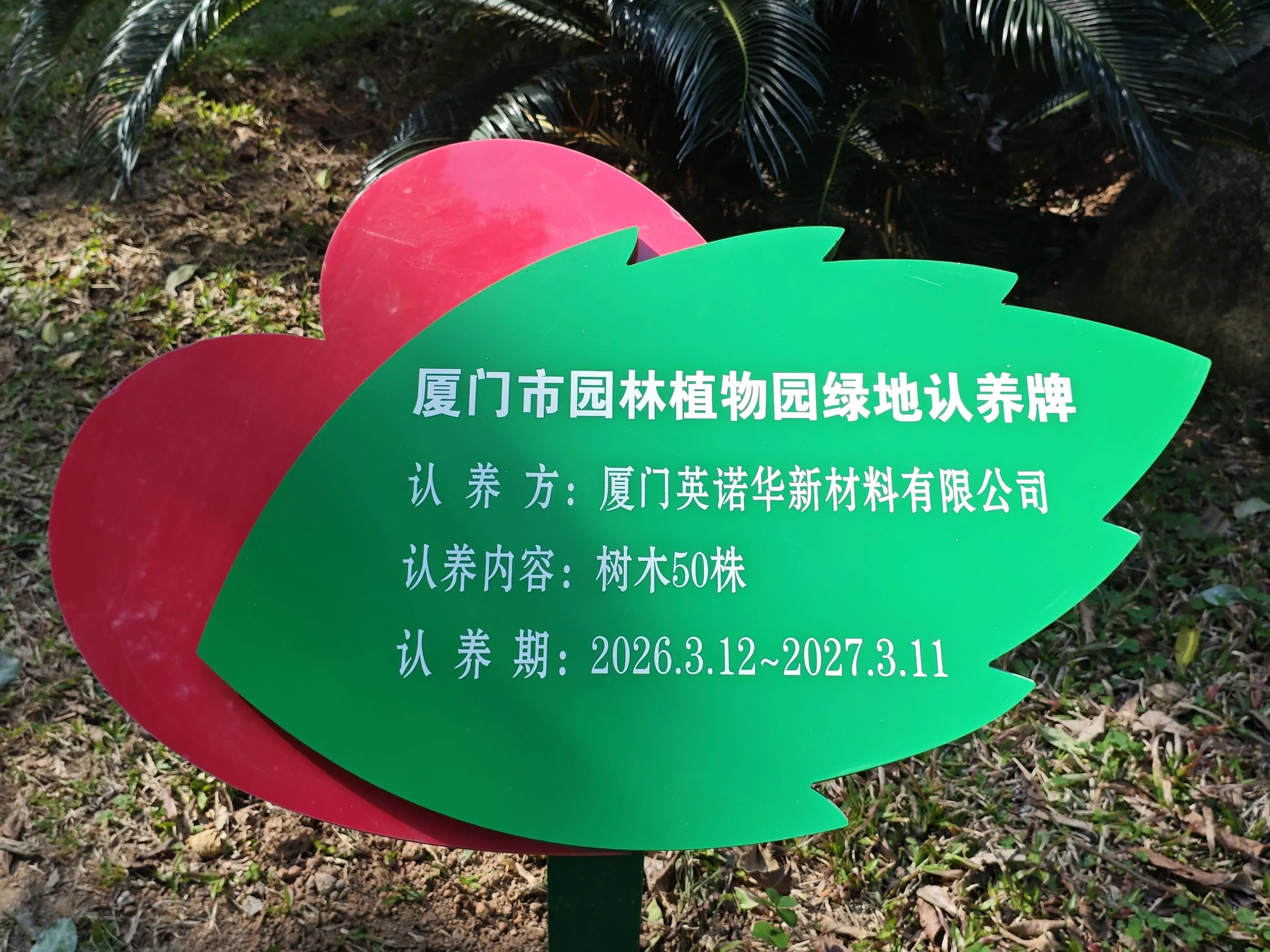
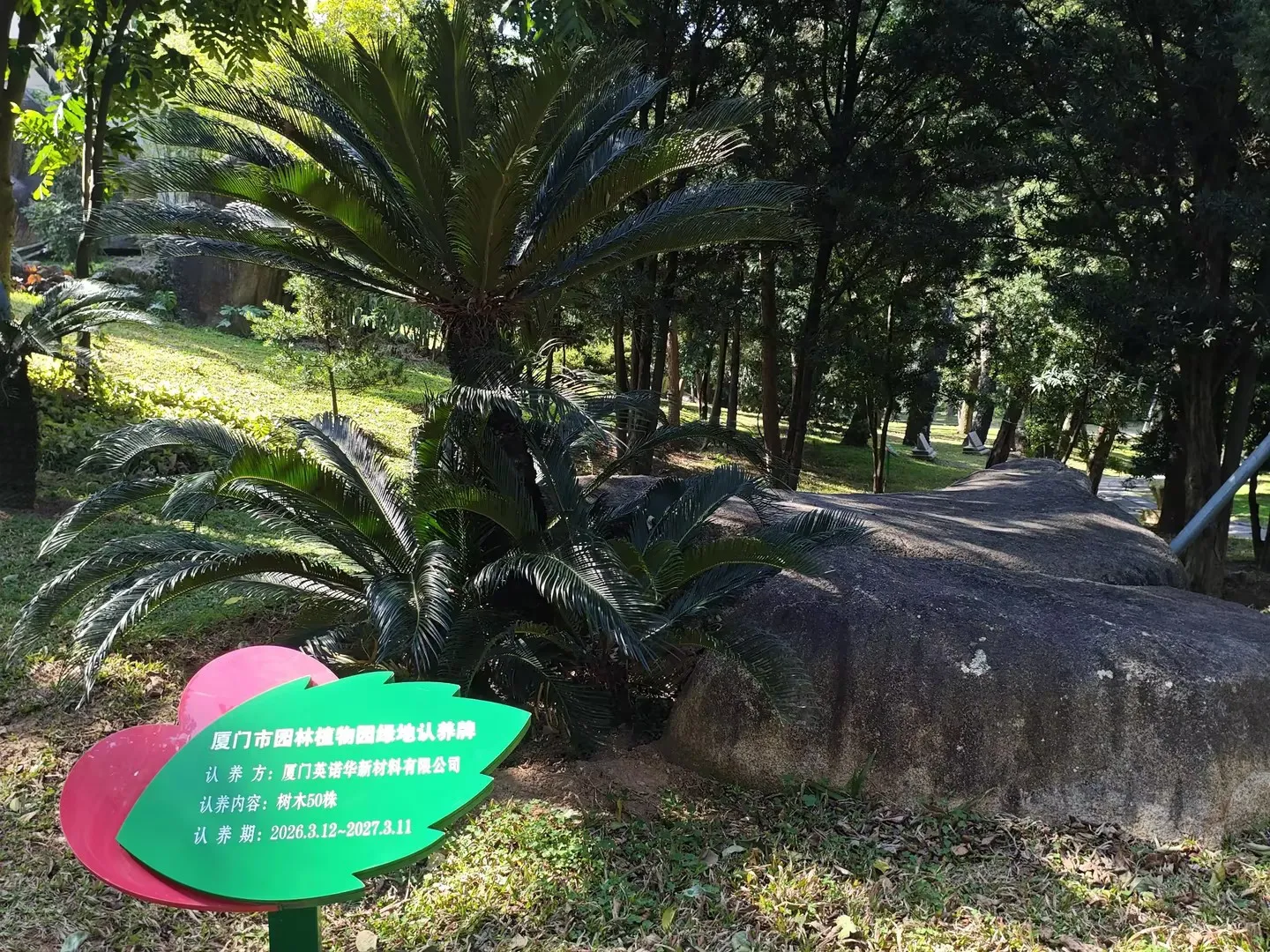
Each tree will have a small adoption tag. No grand ceremony, no camera crews. Just trees gaining a few more people who care, and people gaining a few more trees to watch over.
If philanthropy had personalities, tree adoption would be the slow-burning, devoted kind.
It’s not like a one-time donation. Adoption is more like a relationship: you remember it, you visit, you notice its changes with each season. Did it sprout new leaves in spring? Did the summer storms shake it? When do its leaves turn gold?
More companies are choosing this approach—not because of grand ideals, but because this quiet, enduring care mirrors what responsibility truly means: not a fleeting impulse, but a continuous attention.
In ESG terms, this falls under “environmental responsibility.” Simply put, it means someone in this city genuinely cares for its green life.
From Material Technology to Ecological Responsibility
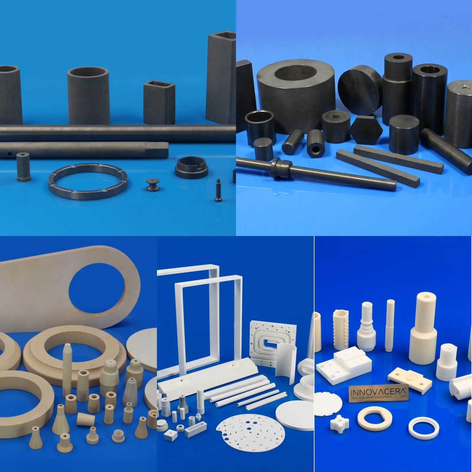
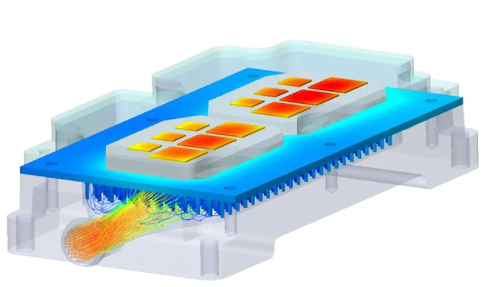
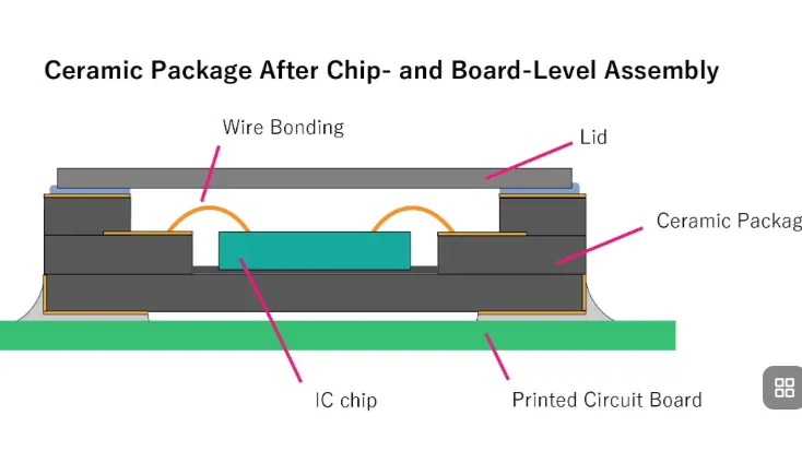
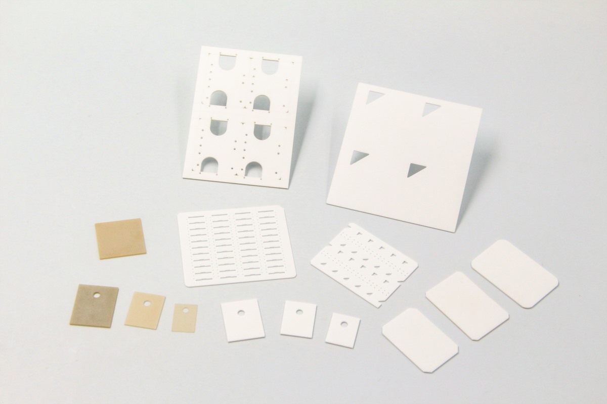
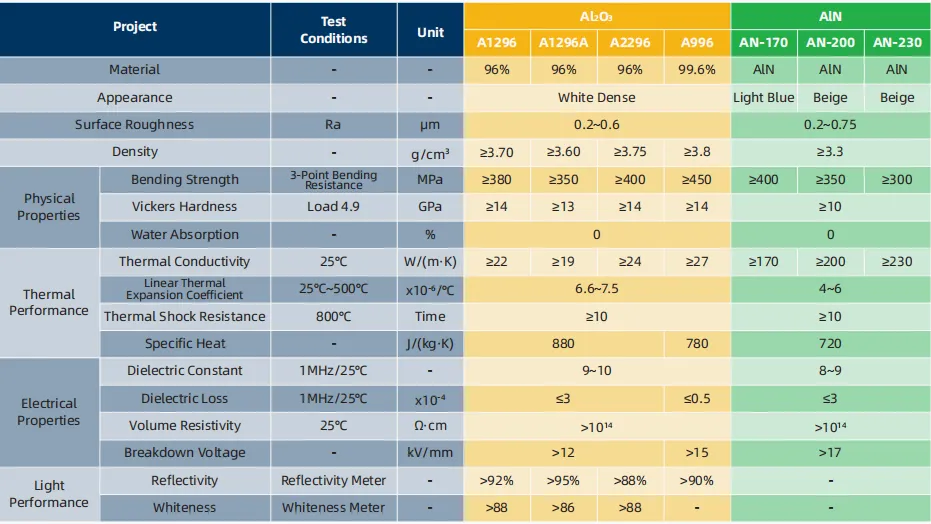
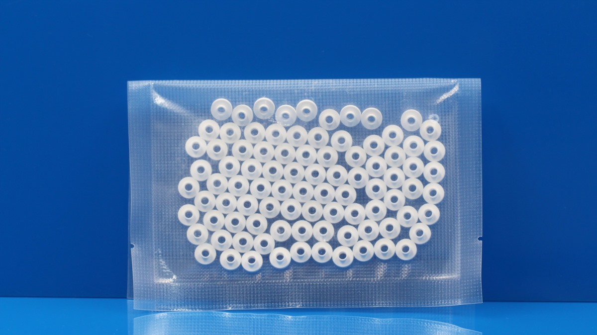
Innovacera specializes in advanced ceramics, precision ceramic materials that withstand high temperatures and high corrosion, and are widely used for semiconductor equipment, vacuum systems, and high-end instrument manufacturing.
It sounds worlds apart from trees. One is industrial, engineered; the other breathes, grows, needs sunlight and time.
But the two share the same logic: both require patience. Materials need stability; so does the environment. Industry pursues precision; ecology seeks balance. On these seemingly parallel tracks, you eventually realize they converge toward the same goal—making life a little better.
Long-Term Practice in ESG
ESG might sound academic, but it is simple things: supporting greening, volunteering for the environment, saving energy, staying engaged over time.
The difference is from one-time actions to ongoing commitments.
Tree adoption fits this trend perfectly: a defined cycle (one year), sustainable involvement (you can follow the trees’ growth), and a real place (the botanical garden). It’s not just a number on a report; it’s a tree you can point to someday and say, “Our company looks after that one.”
Project Details
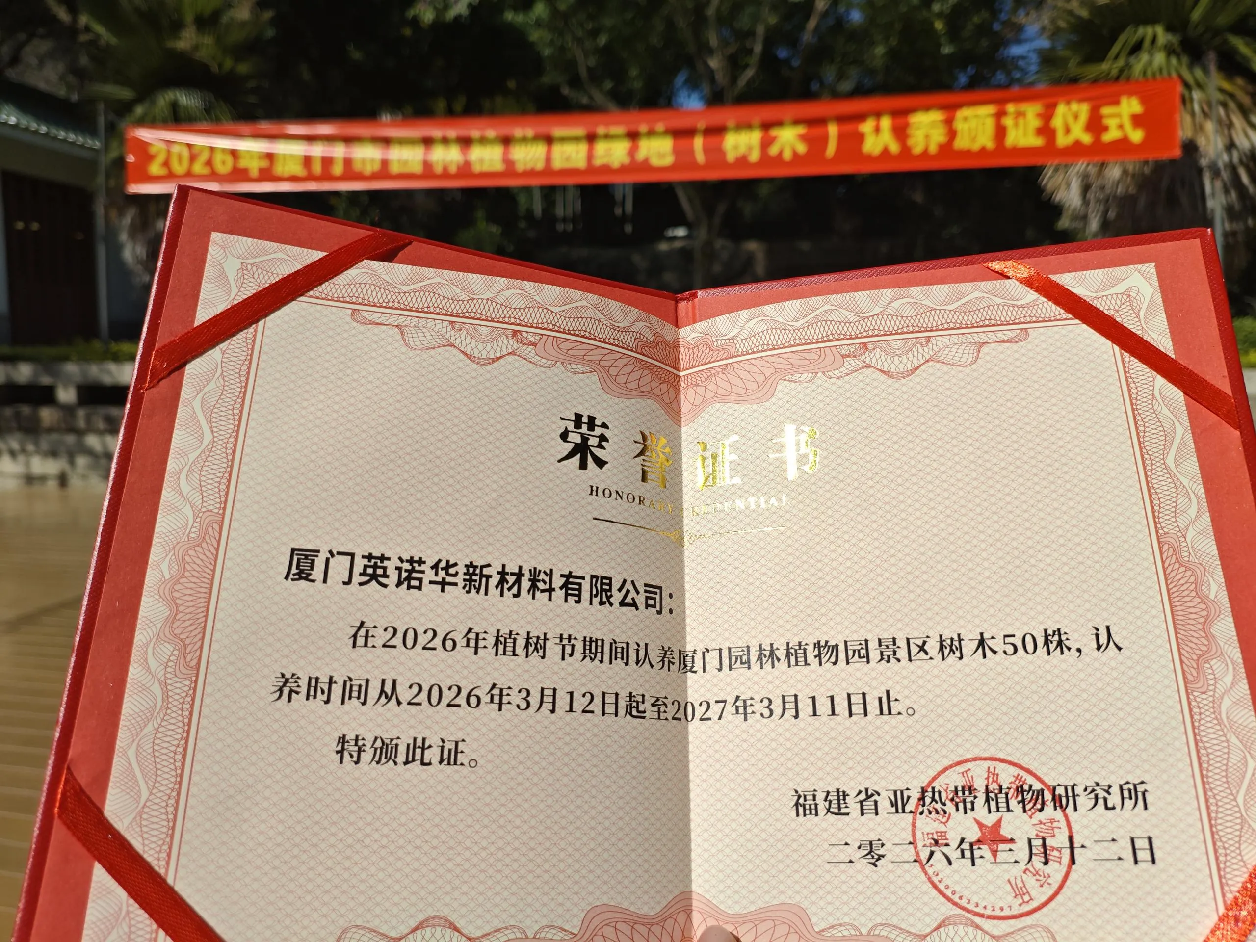
Project Item: Tree Adoption Public Welfare Initiative
Place: Xiamen Botanical Garden
Trees Numbers: 50 trees
Adoption Time: March 12, 2026 – March 11, 2027
Organization: Fujian Institute of Subtropical Botany
FAQ
Why do companies adopt trees?
Because it’s a form of giving that gives back. A donation may not echo, but a tree lives, grows, stands there year after year. For a company, it’s a kind of companionship you can count on.
Does this belong to ESG?
Yes. Environmental responsibility doesn’t have to be grand. Taking good care of a tree is part of it.
Who initiates such programs?
Usually botanical gardens, parks, or ecological protection organizations. They need partners to help safeguard the city’s greenery.
About Innovacera
A Xiamen company specializing in advanced ceramics and precision ceramic components. Its products are widely used in semiconductor systems, vacuum chambers, high-end instruments and more.
In Summary
Maybe someday, when you come to Xiamen Botanical Garden, you’ll notice a tree with a small tag.
That tag is more than just a piece of metal or plastic.
It’s a promise—to remember for a year. And it’s a small, warm connection between 50 trees and a city.
From technology to ecology, from making to caring—a company’s role evolves, but some things remain the same. Like the willingness to wait for a tree to grow.


 Enquiry