technical ceramic solutions

News

Category Archives: News

Direct Bond Copper/DBC Ceramic Substrate For Electronics

DBC Ceramic Substrate Specifications:

  • Material: 96% Alumina + Cu/Ag Coating.
  • Max Size: 138*188mm
  • Thickness: 0.25-1.0mm (0.25, 0.38, 0.5, 0.63, 0.76, 1.0mm).

General Size:

  • 2″*2″(50.8*50.8mm)
  • 3″*3″(76.2*76.2mm)
  • 4″*4″(101.6*101.6mm)
  • 4.5″*4.5″(114.3*114.3mm)
  • 5″*5″(127*127mm)
  • 5″*5.5″(127*139.7mm)
  • 5.4″*7.4″ (138*188mm)

DBC Ceramic Substrate For Electronics

Advantages:

  • Low thermal resistance.
  • Excellent insulation properties
  • Reduce solder layers, lower thermal resistance, reduce cavities, increase the rate of finished products.
  • The super-thin 0.25mm DBC substrate can be substituted for BeO eliminating the problems of environmental pretection and toxicity.
  • Avoid withstand the stress caused by the impact of temperature changes, thus greatly extend the life of semiconductor products.
  • The new packaging and assembly methods can be realized with DBC substrates, it makes the products a higher degrees of integration and volume reduction.
  • The thermal expansion coefficient close to silicon in the semiconductor chip, it can directly solder on the DBC substrate, saving the interface layer Mo plate and then decrease the cost.

Application:

  • Solar-panel array
  • Solid-state relays
  • Electronic heating devices
  • Smartpower building blocks
  • Power Semiconductor Modules
  • Laser Industrial electronics
  • Semiconductor refrig-erators
  • Power control circuits, power hybrids.
  • High frequency switch mode power supplies
  • Telecommunication private branch exchange and receiving system.
  • Building blocks for automobile electronics, the military and aerospace technology.

Notification of INNOVACERA’S Xiamen Office Change 2019

To: INNOVACERA’S Partner

Thanks for your supporting in the past year.

Effective from 18th Jan, 2019, INNOVACERA will change its Xiamen Office as below:

ADD: A506-507,No.7 Yu’nan Fourth Road, Huli District, Xiamen area of China (Fujian) Pilot Free Trade Zone.

Tel: +0086 592 558 9730
Fax: +0086 592 558 9733
Email: sales@innovacera.com

While our office is changing, our business scope, legal status and contact details will remain the same.

We’ll be constantly striving to provide better products and service for you!

The INNOVACERA’S Team


Notification of INNOVACERA’S National Day Holiday

Innovecera office will be closed 1st-8th of October for National Day Holiday.
During this period of time, we have limited access to our e-mail.
We apologize that we are unable to respond to you immediately.
If you require immediate assistance, pls call sales mobile number so that they can solve it soon.
Any advanced ceramic part inquiry, welcome to send to our email.
We will deal with it as soon as we are back in the office.


Zirconia Ceramic Spatula For Mixing Palette Of Dental Application

We got a query requested to develop some ceramic component for mixing palette of dental application, Because customer needs high flexural strength and no contamination
components to get homogenous pastes.

Materials Choose Step (Design Guide)

  • No contamination is the most important
  • Flexural strength
  • Elastic module
  • Fracture toughness

As per the above choice, our engineer recommended Zirconia Ceramic Material for this project.

  • High flexural strength
  • Excellent bending strength
  • Impact resisting
  • Good fracture toughness

Design Solutions

Zirconia ceramic spatula is thickness from 0.3mm to 0.8mm.

zirconia ceramic spatula

zirconia ceramic spatula

Brief Introduction

The zirconia ceramic spatula is used for the mixing palette which dental technicians are working with ceramic powders (for making crowns and bridges). Basically, the ceramic powder is mixed with distilled water. Use the zirconia ceramic spatula for mixing the ceramic powder and the distilled water, it can get homogenous pastes. This zirconia plate is an entire part of a more complex set of tools.

This zirconia spatula had a lot of success on the 2015 biggest dental exhibition(takes place every 2 years in March in Germany).

According to the exhibition publicized, hope this zirconia ceramic spatula will be more widespread use for the dental industry.

Our engineer team will develop various kinds of zirconia or alumina ceramic part for the dental industry, if there is any project enquiry please feel free to get in touch Email:sales@innovacera.com.


Zirconia Ceramic Peg For The Mixing Processing of Food and Beverage Industry

Zirconia Ceramic Peg For The Mixing Processing of Food and Beverage Industry

We got a query requested to develop ceramic milling and mixing components for the processing of the food and beverage industry, cause of the stainless steel occur metal impurities during the milling and mixing processing.

Materials Choose Step (Design Guide)
1. Food Safety
2. Chemical Resistance
3. Wear Resistance
4. Mechanical Strength

As per the above choice, our engineer recommended Zirconia Ceramic Material for this project.
* High Hardness
* Wear Resistance
* Chemical Resistance
* Excellent Mechanical Strength

Design Solutions
Zirconia Ceramic Screw Sleeve bonded with SSL304Shaft (Zirconia Ceramic Beg).

Brief Introduction
The zirconia ceramic peg is a part of a grinding mill machine, which using cerium stabilized zirconia oxide grinding beads (size: 1.6-1.8mm) for grinding mill and mixing processing, so it is requested the grinding pegs had a long life-time and food safety for the processing of food and beverage industry.

zirconia ceramic beg

Our ceramic milling and mixing beg had been using for a year, they are still running and had a good effort.

The next products middle and small zirconia ceramic peg will be coming soon.

Our engineer team will develop various kinds of the ceramic peg, if there is any project enquire please feel free to get in touch Email: sales@innovacera.com.


Looking Back Hannover Messe 2015

On 17 April, the world’s greatest industrial exhibition in Hannover came to an end. INNOVACERA says thank you to everyone who visited and discussed the advanced ceramic project.

INNOVACERA Booth

INNOVACERA Booth

What we show: Advanced ceramic components

With industry solutions, product innovations and services for technical ceramic solutions, our service include as below;

Ceramic Material Solutions

  • Alumina Ceramic;
  • Zirconia Ceramic;
  • Boron Nitride Ceramic;
  • Silicon Nitride Ceramic
  • Machinable Glass Ceramics;
  • Porous Ceramics;
  • Other Advanced Ceramic Material Solutions*;
Alumina Ceramics

Alumina Ceramics

Zirconia Ceramics

Zirconia Ceramics

boron nitride ceramics

boron nitride ceramics

Ceramic Processing

  • Metallization Ceramics
  • Alumina Ceramic Heater
  • Ceramic Metering Pump
  • Ceramic-to-Metal Brazing (Vacuum Interrupter, Vacuum Capacitor, HV Relay)*
  • Ceramic-to-Metal Assembling (Pump Components, Cover Die, Tooling)*
  • Coating, PVD, CVD*

*Cooperate with the Material Research Institute of China

metallized ceramics

metallized ceramics

machniable glass ceramics

machniable glass ceramics

Impressions from the Hannover Messe 2015 in sound and vision

Looking back, we are delighted with the entirely positive feedback from our customers and our many interesting discussions.


Hannover Messe Show

Hannover Messe Show


Brief Introduction of Metallization Ceramics

Brief Introduction of Metallization Ceramics

Advanced ceramics are widely used in electronics and engineering applications for their chemical and mechanical properties. Compared to metals, they are stronger in compression, especially at higher temperatures. Advanced ceramics have good thermal stability (i.e., a low coefficient of thermal expansion) and good thermal and electrical resistance. They are also hard and have excellent dimensional stability.metallized ceramic for vacuum interrupter

As a result, the list of applications for advanced ceramics is including aerospace engine blades, rings and valve components, industrial pump bearings, cutting tools and die parts, medical instruments, and wide uses in the electronics industry as a substrate and in specialized vacuum components.

Metallization ceramics is a famous coating technology in advanced ceramics. They are commonly used in many applications, for example, in power electronics components placed under extreme load, electrical drive engineering, and electrical engineering as well as in electronic components for computer technology.

metallized ceramic component

Key Features

  • Standard Moly-Manganese coatings of .001”+/-.0005” offers a uniform coat and optimum peel strength
  • Standard Nickel plating thickness of .0001”/.0004” creates an ideal surface for vacuum-tight braze seals

Key Benefits

  • Superior bare ceramic and metallization quality
  • Vertically integrated ceramic processing with traceability from the bare ceramic powder through metallization and Nickel plating
  • Application engineering support
  • Specialization in prototype to medium volume with the ability to seamlessly upscale to high volume production if required.

Metallization Capabilities

  • Face metallization of large and small parts
  • Pattern screening of highly intricate details
  • Complete OD metallization
  • Complete ID metallization of even the smallest thru holes
  • Counterbore metallization
  • ID/OD striping to tight tolerance bandwidths
  • Electrolytic and Electroless Nickel plating processes

Typical Applications

  • RF windows
  • Vacuum tubes
  • Laser tubes
  • X-ray Tubes
  • Feedthrough
  • Headers
  • High-power receptacles
  • Insulating discs
  • Insulator rings and cylinders
  • Precipitator products
  • Power switches
  • Traveling wave tubes
  • Power grid tubes

metallized ceramic washer

metallized ceramic tube


Nanomaterials’ grain boundaries absorb defects, lengthen life of nuclear fuel

Nuclear energy supplied 19.4% of the total electricity used in the U.S. in 2013, or 789.0 billion kilowatt-hours, according to the Nuclear Energy Institute. However, the contribution of nuclear to the U.S. grid has been hovering around 19%–20% for the past 25 years.

That stagnation may be partially due to hesitation about the safety and utility of current nuclear fuel cycles, which are at the heart of energy generation in a nuclear power plant.

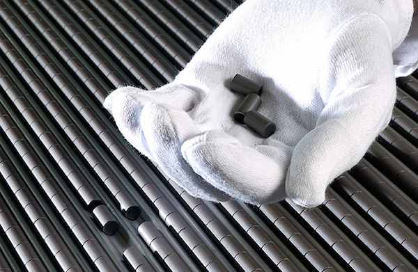
Nuclear fuels come in a variety of forms, many of which are processed into ceramic fuel pellets. The U.S.’s 99 operating reactors consume a lot of pellets—the typical power plant generates 20 metric tons of used nuclear fuel every year—because that fuel must be removed and replaced almost annually within each reactor.

Nuclear fuel pellets are stacked vertically in long metal tubes to power commercial nuclear reactors. There are many steps involved in processing uranium before it is fabricated into nuclear fuel. Courtesy of Areva.

[Check out NEI’s great interactive graphic for more about nuclear fuel production, use, and storage.]

More fuel usage means more upfront costs for new materials and manpower to reload the plant with fresh fuel, but it also means more costs and logistical challenges to safely store spent nuclear fuel, too.

The cost to reload nuclear fuel in a typical 1,000 MWe reactor that refuels on an 18-month cycle is a staggering $40 million, according to NEI. So making fuel last longer can save a lot of money, increase plant efficiency and ouput, and improve safety of nuclear energy. And maybe—just maybe—those changes could push nuclear energy out of that 20% rut.

New research from Ricardo Castro, ACerS member and materials science professor at University of California, Davis, and a team of his colleagues is providing important insight into how nanomaterials behave under irradiation, a finding that may help significantly extend the life of nuclear fuels.

The research, recently published in Scientific Reports, also includes ACerS members John Drazin from UC Davis and Terry Holesinger and Blas Uberuaga from Los Alamos National Laboratory. Additional authors include Sanchita Dey from UC Davis and Yongqiang Wang and James Valdez from Los Alamos.

The team specifically looked at how nanocrystalline nuclear fuels could compare to their microcrystalline counterparts. Although composed of the same material, nanocrystalline and microcrystalline samples are significantly different because they have differing grain sizes, a feature that the team found has a big impact of the material’s properties after irradiation.

0318ctt nuclear fuel rods lo res

Although previous research has suspected that nanocrystalline ceramics would be more radiation tolerant than bulk (microcrystalline) samples of the same material, the team’s newly published research confirms these suspicions and, importantly, provides the mechanism by which it happens—through reduced accumulation of point defects.

Point defects normally form in a material upon irradiation. But accumulation of defects within nuclear fuel negatively affects its behavior and performance, and thus directly impacts its potential life cycle. Decreasing the accumulation of defects, therefore, would increase nuclear fuel lifetime.

Castro and the team studied precisely how defects evolve in response to irradiation, measuring the location and migration of individual defects in microcrystalline and nanocrystalline samples of 10 mol% yttria-stabilized zirconia. According to Castro, the team used zirconia because it has a similar structure to nuclear fuel uranium dioxide.

“We saw very little damage in the nanocrystalline samples, and significant damage in the microcrystalline sample. This is because the grain boundaries in the sample act as sinks for interstitial defects,” Castro says in an email. “That is, nanomaterials accumulate less defects during radiation, being a key element to enhance lifetime of nuclear fuel.”

“Since more defects means to shorter life-time, one can expect longer life for nanocrystalline uranium dioxide fuels as compared to regular micrograined fuels,” Castro says.

Not only was the amount of defects significantly less in nanocrystalline samples, but the type of defects was different, too.


Defects can be gains or losses: gains, or interstitial defects, are crystal structure locations where atoms create spaces that shouldn’t be occupied; losses, or vacancies, are empty atomic seats within the crystal structure that should be filled.


The team found that while microcrystalline samples had both interstitial and vacancy defects, the nanocrystalline samples accumulated only vacancies, which clustered to minimize energy.

Created by Digital Micrograph, Gatan Inc.


This distinction provides important insights into the mechanisms of defect reduction in these materials.


“In nanocrystalline samples, the probability of the defect ‘finding’ a boundary is much higher because grains are smaller,” Castro explains. “Boundaries are stable sinks for the interstitials, but produced vacancies are shared between boundary and bulk, since they can form metastable clusters in the bulk. Therefore, in nanocrystalline samples, one cannot find interstitial defects in the crystal—only vacancies. In the microcrystalline samples, we find both, and in much higher concentrations (since only a few defects can actually find a boundary).”


Confirming that the boundaries were indeed acting as sinks to absorb the defects in nanocrystalline samples, the scientists measured grain growth in nanocrystalline samples only following irradiation.


Castro explains that the amount of radiation they exposed the test materials to was equivalent to 4.5 years of service life in reactors, despite the fact that nuclear fuels are typically replaced within one year in real life due to damage considerations and safety precautions.


“Since zirconia also finds structural applications, the results can also be used to predict nanoeffects in [nuclear fuel storage conditions, too,] such as core barrels and dry casts. The core barrel radiation equivalent is about 84 years. As a reactor vessel, the tested radiation would be equivalent to 21 million years. So again, nanomaterials would be able to resist much longer than microcrystalline samples.”


The open-access paper is “Radiation tolerance of nanocrystalline ceramics: Insights from yttria stabilized zirconia” (DOI: 10.1038/srep07746).

Oringinal Link


H.C. Starck Introduces MoNb and MoW Sputtering Targets at FPD China 2015

H.C. Starck is taking innovation to a new level with its hottest new sputtering alloys for Touch Screen Panel (TSP) applications. Curved and flexible touch screens are the latest in HDTV, smart phones, tablets and mobile device technology.

Touch screens use H.C. Starck’s molybdenum-niobium (MoNb) targets to sputter thin films for barrier, capping and conducting layers in these devices.

The MoNb alloy enables higher sputtering rates, higher quality film with fewer defects and world-class corrosion resistance. Production of single piece targets is H.C. Starck’s distinct advantage. Another key advantage is the higher relative density found in extruded targets compared to Hot Isostatic Press (HIP) targets. Second to none is H.C. Starck’s best-in-class extrusion process that produces a diverse portfolio of materials, shapes, sizes and lengths.

H.C. Starck’s molybdenum-tungsten (MoW) planar targets are applied when forming gate and touch sensor layers for TFT- LTPS and in-cell type touch panels. H.C. Starck offers varying compositions for single piece length tiles based on customer requirements. Thin films produced from MoW targets have excellent wet and dry etching characteristics.

H.C. Starck’s newest product line of molybdenum based alloys showcases the company’s ability to customize alloys for electrical performance, corrosion resistance and etch characteristics for higher reliability in TSP applications. These alloys feature large size capabilities with rotary targets up to 4100mm long, planar targets up to Gen 5 in size as well as segmented (or tiled) targets.

”We are very excited about the latest advancements in touch screen technology,” said Dmitry Shashkov, Member of H.C. Starck’s Executive Board and Head of the Fabricated Products Division. “The evolving technology in TSP applications such as flexible touch screen devices necessitates higher performance and durability. H.C. Starck’s expertise in sputtering target materials and rapid product development can offer TSP customers the capabilities for improved system performance and cost.”

Development of these innovative alloys is enabled by H.C. Starck’s expertise in thin film characterization and ESBD analysis of textures. Customized alloy development utilizes the unique processing of refractory metals, including powder metallurgy processing, high temperature rolling, extrusion and rotary forging.

H.C. Starck is pleased to exhibit again at this year’s FPD China 2015,17-19 March, Shanghai New International Expo Center in China, Booth N1-1563. Visit with our experienced technical staff to learn how our leading-edge products and technical support could contribute to your success in competitive touch screen applications.


Centorr Vacuum Industries Sells Two High-Temperature Furnaces for Aluminum Nitride Production

Centorr Vacuum Industries announced it has shipped orders for two high-temperature sintering furnaces for 2015 delivery to a leading firm in the production of AlN substrates for the LED market in China.

The designs include CVI’s 2 cu ft graphite furnace for AlN sintering and a refractory metal furnace rated to 1850C for a secondary heating process. These new furnaces build on the success of CVI’s experience in non-oxide ceramics and include modifications made specifically for high-temperature sintering of advanced ceramics.

Centorr’s graphite furnace design includes robust Graphite Tube and Block elements designed for use to 2250°C, with a 4-sided hot zone and integral graphite retort for excellent temperature uniformity. The rigid graphite insulation design provides for long-term service even in the presence of process off-gassing and residual binder contamination, while the new dual-flow Sweepgas® system allows more effective “sweeping” away of the process offgassing. Furnace control is via PLC/Programmable Controllers with Centorr’s custom-designed HMI visualization interface.

Centorr Vacuum Industries Sintervac Non-Oxide design is available in sizes of 2,3,4.5,9,16,24, and 54 cubic foot volumes. The refractory metal furnace design, sized at 1 cu ft will be used for a specific part of the AlN process where a non-graphite hot zone is desired for material cleanliness. The system is rated to 1850C and offers temperature uniformity under +/- 3°C.

Centorr Vacuum Industries is a high temperature vacuum and controlled atmosphere furnace manufacturer with an installed base of over 6500 units worldwide. Their furnace offering ranges from large commercial and production units with hot zones over 3m x 3m, to smaller Lab and Research & Development furnaces for use at temperatures over 3500°C. They are located in Nashua, NH with a fully staffed Aftermarket Field Service group, and Applied Technology Center offering R&D support and toll production service.

SourceLink: Centorr Vacuum Industries


Enquiry