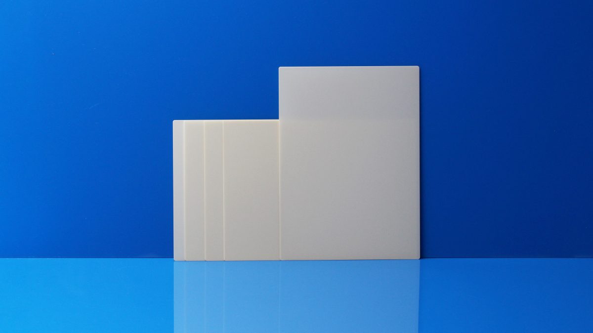
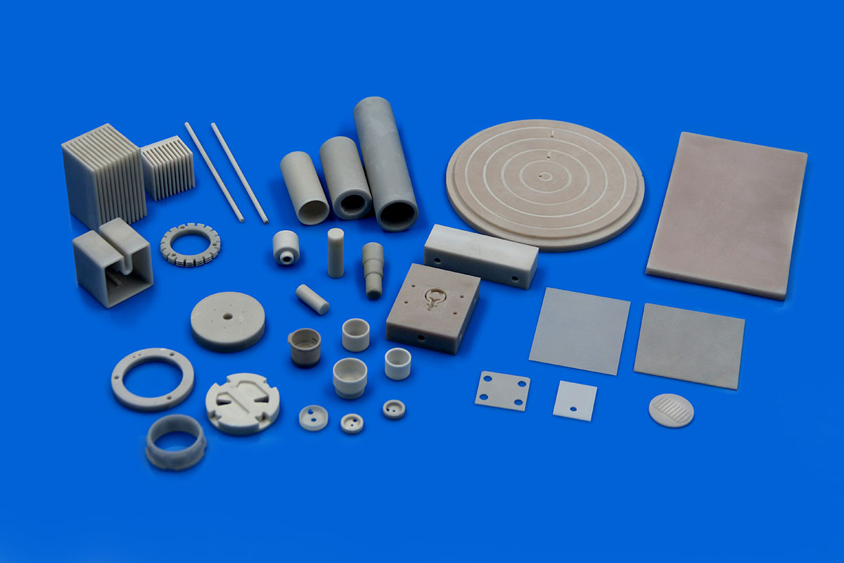
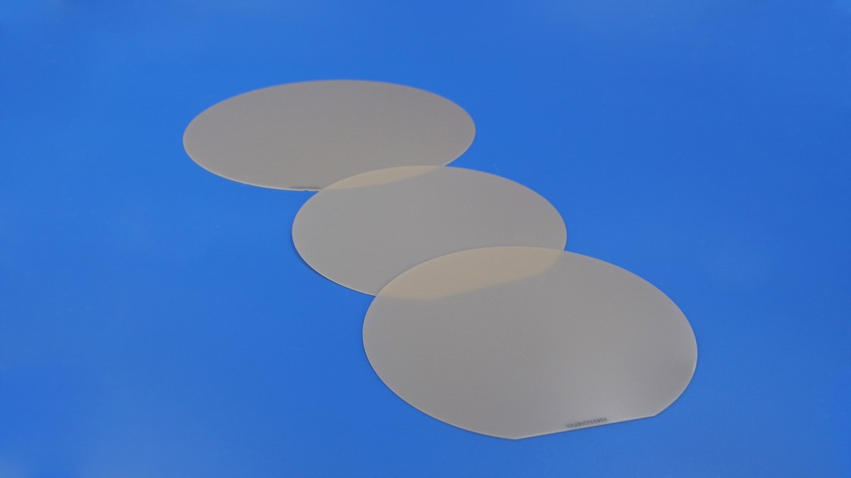
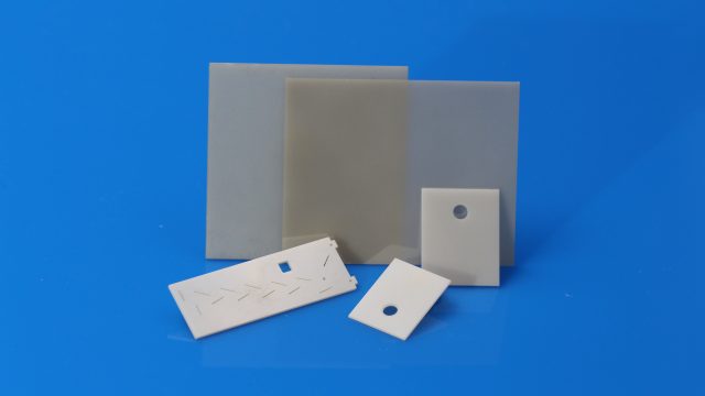
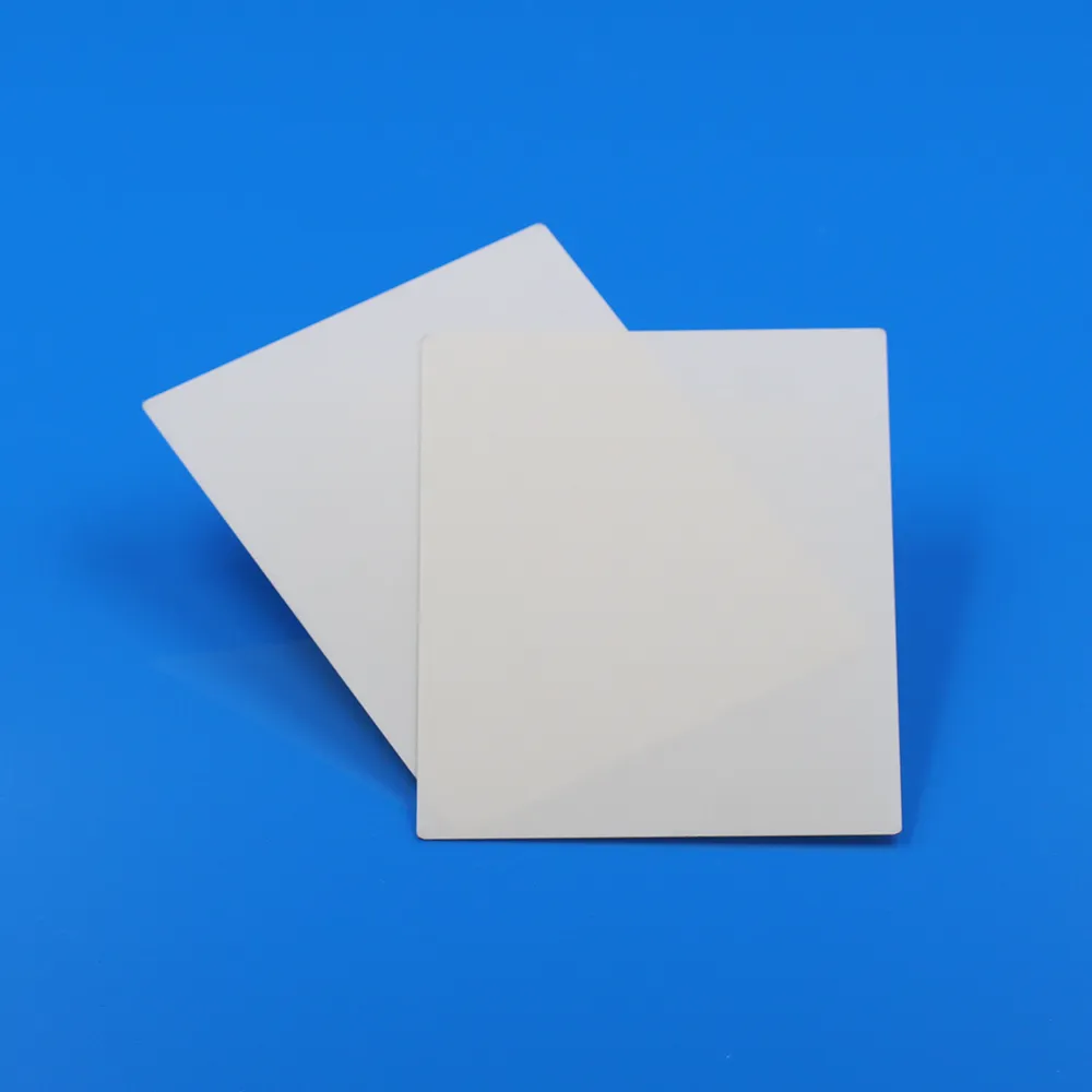
When a DPC foundry loads a 138 × 190 × 0.635 mm aluminum nitride panel into a sputtering chamber, the ceramic is no longer just a material purchase — it becomes a process variable. Surface roughness determines whether the seed layer adheres uniformly. Warpage determines whether the panel sits flat against the carrier during photolithography. Batch-to-batch dimensional drift determines whether downstream laser scribing yields stay predictable across a production quarter.
Buyers sourcing large-format Aluminum nitride (AlN) Substrates for metallization, thick-film printing, thin-film deposition, or precision laser cutting often focus heavily on thermal conductivity as the headline specification. In practice, the parameters that most directly control your process yield are surface condition, flatness, and consistency — not conductivity alone.
This article maps those critical specifications to specific downstream processes, identifies the decision logic behind each tolerance, and flags the evaluation questions worth raising with any substrate supplier.
Why 138 × 190 mm Is a Process-Relevant Panel Size
The 138 × 190 × 0.635 mm format is not an arbitrary dimension. It corresponds to a panel footprint that allows multiple finished sub-pieces to be processed in a single sputtering or printing pass, then singulated by laser or dicing saw into smaller substrates. The economics depend on maximizing usable die per panel while keeping defect rates at the edges and across the field within acceptable limits.
This means the specifications that matter are field-level, not just nominal:
- Surface roughness (Ra) must be consistent across the full 138 × 190 mm face, not just at the center.
- Warpage must be measured as total indicator reading (TIR) across the longest diagonal, not at a single point.
- Thickness uniformity across the panel affects both metallization coverage and sintering deformation in thick-film processes.
- Edge condition — chip size, edge straightness, corner integrity — affects cutting yield when the panel is later singulated.
Understanding which specification governs your process is the first decision to make before issuing a purchase order.
Surface Roughness: What Each Process Actually Requires
DPC (Direct Plated Copper) Sputtering and Plating
In DPC processing, a titanium or chrome adhesion layer is sputtered onto the AlN surface before copper is deposited. Adhesion depends on intimate contact between the metal atoms and the ceramic surface. If the Ra is too high, the peaks and valleys create microscopic voids under the seed layer, leading to delamination under thermal cycling. If the Ra is too low — a mirror-like surface — chemical adhesion can also be compromised depending on the specific process chemistry used.
A typical working range cited in DPC process development is Ra in the region of 0.2–0.6 µm for as-fired or lapped AlN, though the appropriate value depends on the specific sputtering parameters and adhesion chemistry of each foundry. The key buyer question is not ‘how smooth is it?’ but ‘does the Ra specification match the bonding window my sputtering process was qualified on?’
Additionally, surface cleanliness — absence of organic contamination, particulates, or residual sintering aids — is equally important. Suppliers should be able to confirm the cleaning protocol applied before packaging.
Thick-Film and Hybrid Circuit Manufacturing
Screen printing of resistive or conductive pastes onto AlN is sensitive to surface texture in a different way. A surface that is too rough causes paste to bleed into micro-channels between grains, affecting line definition. A surface that is too smooth may reduce mechanical keying of the fired paste, potentially reducing bond strength after sintering.
Thickness uniformity across the panel becomes critical here because paste volume deposited per stroke is a function of the gap between the screen and the substrate surface. If the panel has a bow or a thickness gradient, the printed line width and thickness will vary across the field, introducing resistance variation before the laser trimming step.
For thick-film work, buyers should specify both Ra and total thickness variation (TTV) across the panel, not just a nominal thickness value.
Thin-Film Deposition and Laser Trimming
Thin-film processes — evaporation, CVD, or advanced sputtering for precision resistor networks — are the most sensitive to surface condition of any of the downstream applications. Sub-angstrom-level film uniformity can be disrupted by surface asperities in the Ra > 0.4 µm range. Buyers in this segment typically specify tighter Ra tolerances and may require a lapped and polished surface rather than an as-fired surface.
Laser trimming of deposited resistors adds a second sensitivity: the substrate must be dimensionally stable during the trim pass. Any residual stress that causes the panel to shift position or flex under laser thermal load will move the trim kerf relative to the resistor geometry.
Warpage: The Specification Most Often Under-Specified
Warpage in large-format AlN substrates arises from two sources: sintering-induced stress gradients and post-sintering handling. Both are manageable through process control, but both are also easy to obscure when a supplier reports only a nominal flatness value without specifying the measurement method or the sample size of the inspection.
How Warpage Affects Downstream Processes
- Sputtering and CVD: Most substrate holders or carrier plates assume a flat substrate. A panel with warpage exceeding the holding mechanism’s compliance range will not be held uniformly, leading to thickness gradients in the deposited layer and potential film stress differences across the field.
- Screen printing: A bowed panel creates variable snap-off distance, which changes paste transfer volume across the panel. The result is printed conductor thickness variation that cannot be compensated by paste rheology alone.
- Laser processing: For laser scribing or cutting, warpage shifts the focal plane. If the substrate surface height varies by more than the depth of focus of the laser optic, cut quality degrades toward the panel edges. This is a direct yield driver for singulation operations.
- Vacuum chucking: Many precision processes use vacuum chucks to hold the substrate. A panel with excessive warpage will either fail to seal on the chuck or will be mechanically forced flat, introducing internal stress that may cause cracking during subsequent thermal steps.
What to Specify and How to Verify
Warpage for large panels should be expressed as a maximum bow value in microns or as a bow-to-length ratio (e.g., µm/mm) measured over the full diagonal. A supplier reporting ‘flatness ≤ X µm’ without specifying whether this is measured at the center or across the full field is providing incomplete information.
Buyers should ask:
- Is warpage measured on 100% of panels, or on a sampling basis?
- What is the measurement fixture — free-standing, vacuum-chucked, or gravity-supported?
- What is the pass/fail threshold, and what is the typical distribution within the specification?
Batch-to-batch consistency of warpage data — not just the single-panel spec — is the correct quality metric for production purchasing decisions.
Thickness Uniformity and Its Relationship to Both Parameters
Surface roughness and warpage are easier to evaluate in isolation, but both are influenced by a third variable: thickness uniformity. A panel with high TTV (total thickness variation) may appear to meet an Ra spec at any single measurement point while still having systematic surface height differences across the field that behave like large-scale roughness from the perspective of a sputtering process.
For 0.635 mm nominal thickness, a reasonable TTV specification for DPC and thin-film applications is typically in the range of ±0.025 mm or tighter, but the appropriate value depends on the specific chuck or carrier design used in the buyer’s process. Buyers should confirm TTV requirements with their process engineering team before specifying to a supplier.
Edge Quality: Underrated for Cutting Yield
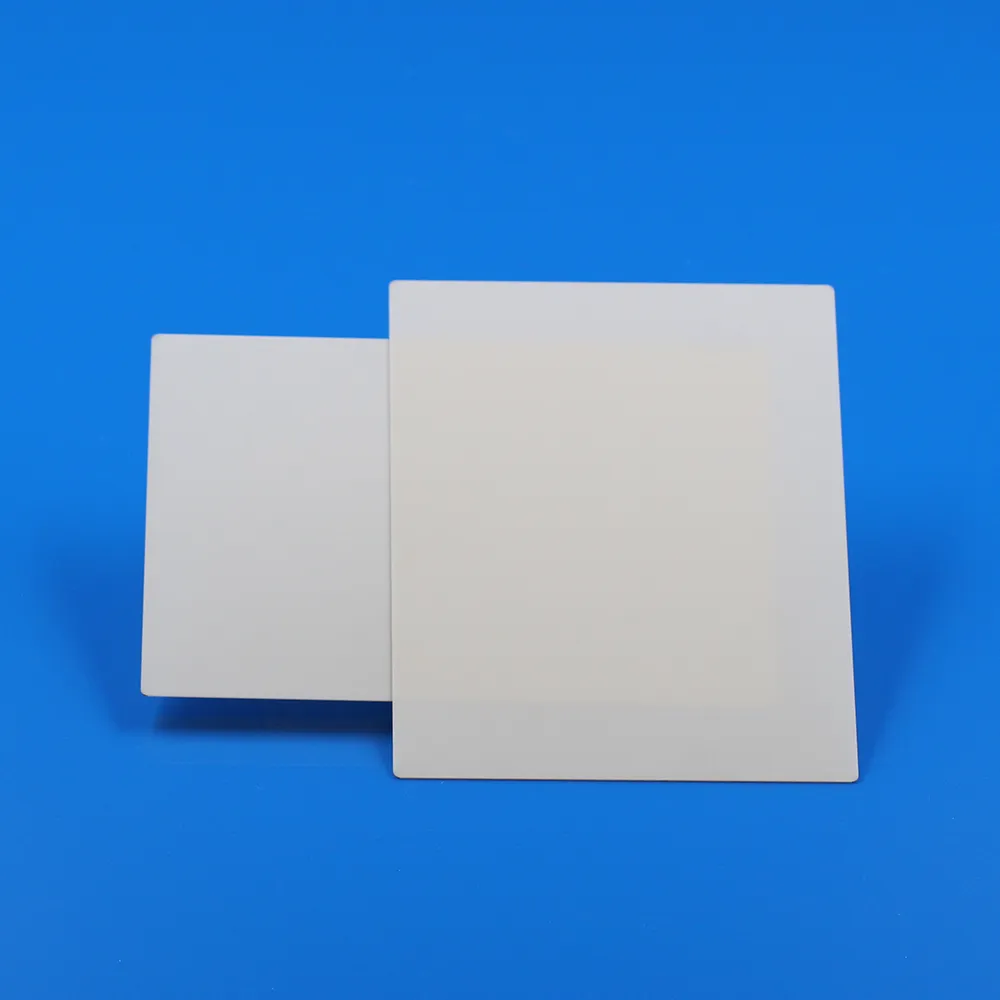
For buyers who purchase large AlN panels specifically for subsequent laser cutting or dicing into smaller pieces, the edge condition of the as-received panel has a direct effect on singulation yield. Edge chips, microcracks propagating inward from the panel perimeter, or poor edge straightness all create initiation sites for crack propagation during dicing.
The usable area of the panel — after accounting for an edge exclusion zone that avoids perimeter defects — affects the number of good sub-pieces per panel. A supplier that holds tighter edge quality specification allows the buyer to reduce the edge exclusion margin and extract more usable pieces per panel.
Ask suppliers to specify: maximum edge chip depth, edge straightness tolerance, and whether corners are chamfered or left as-cut.
Batch Consistency: The Specification That Doesn’t Appear on a Datasheet
For any buyer running a qualified production process, the most commercially significant quality attribute is not the best panel in a shipment but the worst panel in a shipment — and whether the worst panel in shipment 47 is comparable to the worst panel in shipment 12.
Batch consistency encompasses:
- Lot-to-lot variation in Ra (can affect sputtering adhesion qualification)
- Lot-to-lot variation in warpage (can affect chuck seating in automated lines)
- Lot-to-lot variation in surface chemistry (relevant to cleaning and activation steps)
Production buyers should request CPK data or at minimum a multi-lot statistical summary for the key dimensions — not a single-lot certificate of conformance. Suppliers with IATF 16949 certification have the process discipline infrastructure to support this kind of data request, though whether any specific supplier actually tracks and shares it is a question to verify directly.
Packaging and Incoming Inspection
Large AlN panels are fragile. A 138 × 190 × 0.635 mm substrate with a nominal flexural strength of several hundred MPa is still susceptible to edge chipping from vibration during transit if inter-leaf protection is inadequate. For cleanroom-destined substrates, particulate contamination introduced during packaging is as damaging as surface contamination introduced during sintering.
Ask suppliers about:
- Inter-leaf material type and cleanliness classification
- Orientation of panels in the shipping box (flat-stack vs. vertical)
- Humidity control during packaging (relevant for hygroscopic packaging materials that could introduce moisture-related surface chemistry changes)
For DPC and thin-film buyers, confirming that the supplier’s packaging protocol is compatible with your incoming inspection and cleaning procedure is worth the early-stage conversation.
Evaluation Questions for Supplier Qualification
The following questions translate the technical discussion above into a practical supplier evaluation checklist:
- What is the specified Ra range (not just maximum), and over what measurement length? A single Ra value without measurement length context is incomplete.
- How is warpage measured — free-standing or fixtured — and is 100% inspection or sampling performed?
- What is the TTV specification, and what method is used to measure it across the full panel?
- What is the edge chip maximum depth and edge exclusion zone recommendation?
- Can you provide multi-lot dimensional data (not just a single CoC) to support process qualification?
- What cleaning and packaging protocol is used, and what cleanliness level is guaranteed at point of shipment?
- What is the minimum order quantity, and what is the standard lead time for production quantities? (Relevant primarily for laser cutting and precision cutting buyers who need inventory availability.)
Procurement Considerations
Large-format AlN substrates in the 138 × 190 mm panel format are process inputs, not commodities. The specifications that govern yield in DPC sputtering, thick-film printing, thin-film deposition, and laser singulation are surface roughness, warpage, thickness uniformity, edge quality, and batch-to-batch consistency — in that order of process sensitivity, depending on the application.
Buyers who specify only thermal conductivity and nominal dimensions will encounter process variability that is difficult to trace back to the substrate because the relevant parameters were never contractually defined. The correct approach is to specify Ra range (not just maximum), warpage as a full-panel TIR measurement, TTV across the diagonal, and to request multi-lot statistical data before committing to a production supplier.
Suppliers who can provide that data transparently, and who have the process control infrastructure to maintain it lot after lot, are the appropriate counterparties for production-scale purchasing — regardless of where they are located.
Discuss Your AlN Substrate Requirements
Looking for large-format AlN substrates with controlled surface roughness, warpage, and thickness consistency? Send your drawings, target specifications, and downstream process requirements to sales@innovacera.com. Our team will review your application and help identify a suitable substrate specification for evaluation.