In high-tech fields such as electronics, new energy, ceramic substrates serve as crucial support and heat dissipation materials, and their processing precision directly determines the performance and reliability of end products. Laser processing technology, with its advantages of non-contact operation, high precision, and small heat-affected zone, has become the preferred process for precision manufacturing of ceramic substrates. This article comprehensively analyzes the technical capabilities and application value of laser processing for ceramic substrates based on actual processing tolerance data.
I. Laser Processing: The Optimal Solution for Precision Manufacturing of Ceramic Substrates
Ceramic materials are characterized by high hardness, high brittleness, and high temperature resistance. Traditional machining is prone to defects such as chipping and cracking. However, laser processing technology uses photon energy to achieve precise material removal, which perfectly solves the technical pain points of ceramic processing.
1.1 Advantages of Laser Processing Technology
Non-contact processing: Avoids ceramic cracking caused by mechanical stress, increasing the yield rate to over 99%.
High-precision control: Positioning accuracy can reach the micrometer level, meeting the assembly requirements of precision electronic components.
Flexible production: Processing patterns can be quickly switched via a program to adapt to multi-variety, small-batch production.
Small heat-affected zone: The temperature is concentrated in the processing area, and the properties of surrounding materials are not affected.
1.2 Scope of Core Processing Capabilities
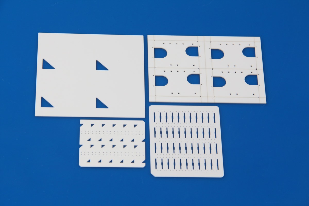
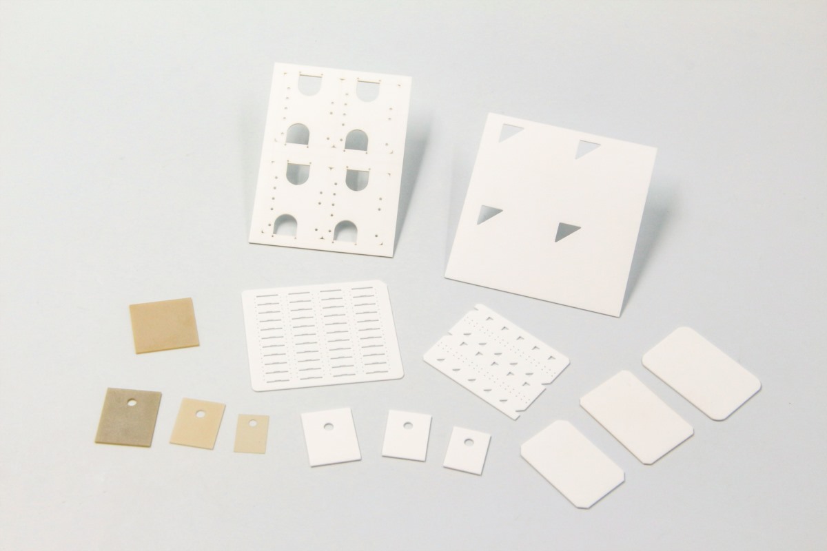
– Laser processing technology enables the comprehensive precision manufacturing of ceramic substrates, covering:
– Substrate shape cutting (rectangular, irregular shape)
– Micro-hole machining (minimum hole diameter down to 0.08mm)
– Grooving (minimum groove width 0.08mm)
– Machining of positioning holes (positional tolerance ±0.03mm)
II. Detailed Explanation of Precision Parameters for Laser Processing of Ceramic Substrates
Based on actual production data, laser processing of ceramic substrates demonstrates superior precision in dimensional control. The following is a detailed tolerance parameter table, covering both standard processing and extreme precision application scenarios.
2.1 Machining Accuracy Parameter Table
| Processing category | Standard tolerance (mm) | Limit tolerance (mm) | Technical features |
| substrate length and width | ±0.15 | ±0.05 | Meets the assembly tolerance requirements of most electronic devices. |
| Hole position | ±0.05 | ±0.03 | High-precision positioning ensures accurate component docking. |
| Small aperture (φ < 0.8 mm) | ±0.1 | ±0.05 | Suitable for processing miniature heat dissipation holes and through holes |
| Medium diameter (φ0.8~2.5mm) | ±0.1 | ±0.08 | Common specifications that balance accuracy and processing efficiency |
| Large aperture (φ>2.5mm) | ±0.15 | ±0.13 | Meets the installation requirements of large components |
| Minimum aperture | – | 0.08 | Breaking through the limits of traditional processing, achieving the manufacturing of ultra-micro holes. |
| Minimum slot width | – | 0.08 | Suitable for machining fine circuit grooves and fluid channels |
| Minimum fillet radius | – | 0.5 | Reduce stress concentration and improve substrate structural stability |
| Hole edge spacing | >Substrate thickness | >0.5 | Ensure substrate strength and prevent cracking in the processing area. |
3. Market Application Prospects
Driven by emerging industries such as new energy vehicles, 5G communications, and artificial intelligence, the market demand for high-precision ceramic substrates will continue to grow. Laser processing technology, as a core manufacturing process, will play a crucial role in the following aspects:
– Ceramic substrate manufacturing for power modules in new energy vehicles
– Processing of packaging substrates for next-generation semiconductor devices
– Precision ceramic component production for micro medical devices
Conclusion
Laser processing technology for ceramic substrates, with its superior precision control, flexible processing methods, and wide material adaptability, has become a core technological support for high-end ceramic manufacturing. From positional tolerances of ±0.03mm to the processing of ultra-micro holes of 0.08mm, breakthroughs in every precision parameter have propelled the electronics and information industry towards higher precision, miniaturization, and greater reliability. With continuous technological innovation, laser processing will continue to play a crucial role in the field of ceramic substrate manufacturing, providing strong technical support for the development of high-end manufacturing.
Declaration: This is an original article of INNOVACERA®. Please indicate the source link when reprinting: https://www.innovacera.com/news/laser-processing-of-ceramic-substrates-a-core-technology-supporting-high-precision-manufacturing.html.
 Substrates")
 Substrates")
 Substrates")
 Enquiry