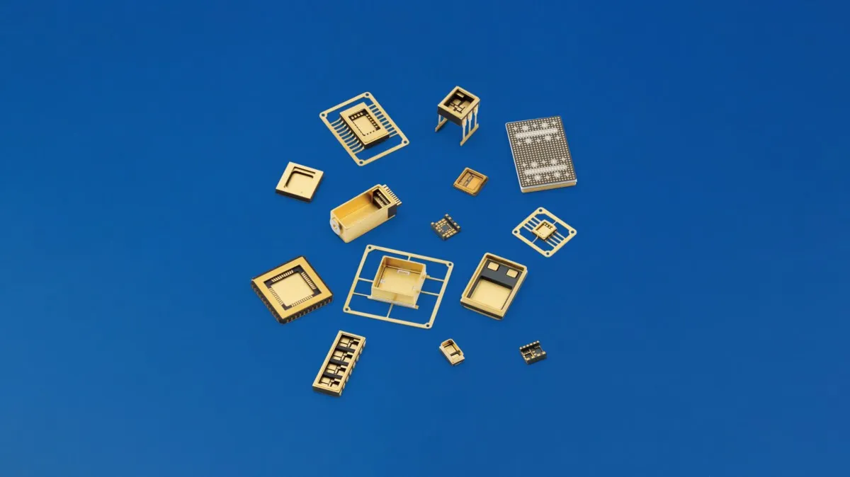
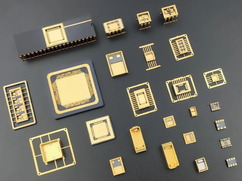
Ceramic packaging is the “housing” for sealing and protecting semiconductor chips, MEMS, or other electronic components. This effectively protects Integrated circuit packaging (ICs), sensors, and other electronic devices from external environmental influences such as moisture, dust, and temperature fluctuations. As semiconductor technology advances towards higher power, smaller size, and higher frequency.
A ceramic package consists of a multilayer ceramic substrate, metal paste and a metal lid, which is made of High-Temperature Co-Fired Ceramic (HTCC) process. The core strength of this method lies in leveraging the superior physical properties inherent to ceramic materials. The ceramic materials are alumina (Al2O3) or aluminum nitride (AlN), possess excellent thermal conductivity, high electrical insulation, and superior mechanical strength.
Our ceramic hermetic packages deliver consistently high performance in leakage rates lower than 5×10⁻⁸ atm·cc/s range. And brazed construction provides excellent mechanical reliability for use in microelectronic packaging designs that meet performance standards.
Features of Innovacera’s Ceramic Packages
– Abundant Material Options
Innovacera offers a wide variety of ceramic materials, such as Al2O3 and AlN, to achieve your performance requirements, with superior thermal conductivity, high-frequency, and coefficients of thermal expansion characteristics.
– Flexible Design Options
Innovacera’s process involves laminating many layers of ceramic. It facilitates lower inductance, miniaturization, cavity structures, and designs a cavity for any chip, with limitless freedom in terminal arrangement.
– Electrical Properties
Three-dimensional electrical routing and structures make it possible to design for specific electrical properties.
– Thermal Properties
(1)Coefficient of Thermal Expansion: We can offer materials with coefficients of thermal expansion closely matching the semiconductor chip. Ceramics do not warp easily, even when heated, thus stabilizing device properties.
(2)High thermal conductivity: We can offer materials with excellent heat dissipation.
– Mechanical Characteristics
As package materials, ceramics offer superior properties of strength, stability, rigidity, and Young’s Modulus.
– Ceramic packaging supports many chip- and board-level assembly options.
(1)Chip-level assembly options include wire bonding and flip-chip bonding.
(2)Board-level assembly options include QFP, PGA, DIP, LCC, and others.
Innovacera is committed to continuously refining its materials and assembly processes, striving to provide stronger assurance for chip applications across diverse industries. Looking forward contact our photonic packaging engineering team today to discuss your application-specific requirements.
Declaration: This is an original article of INNOVACERA®. Please indicate the source link when reprinting: https://www.innovacera.com/news/what-is-ceramic-packaging-a-guide-to-hermetic-protection-for-semiconductors.html.

")

 Enquiry