Soldering ceramic vacuum welding components: A long-term and reliable sealing solution for high vacuum systems
In high vacuum and ultra-high vacuum systems, the electrical connections or functional components crossing the vacuum boundary are always the key factors affecting the stability and lifespan of the system. Traditional organic seals or mechanical compression structures often encounter risks of aging, gas release and sealing failure under high temperature, thermal cycling and long-term operation conditions.
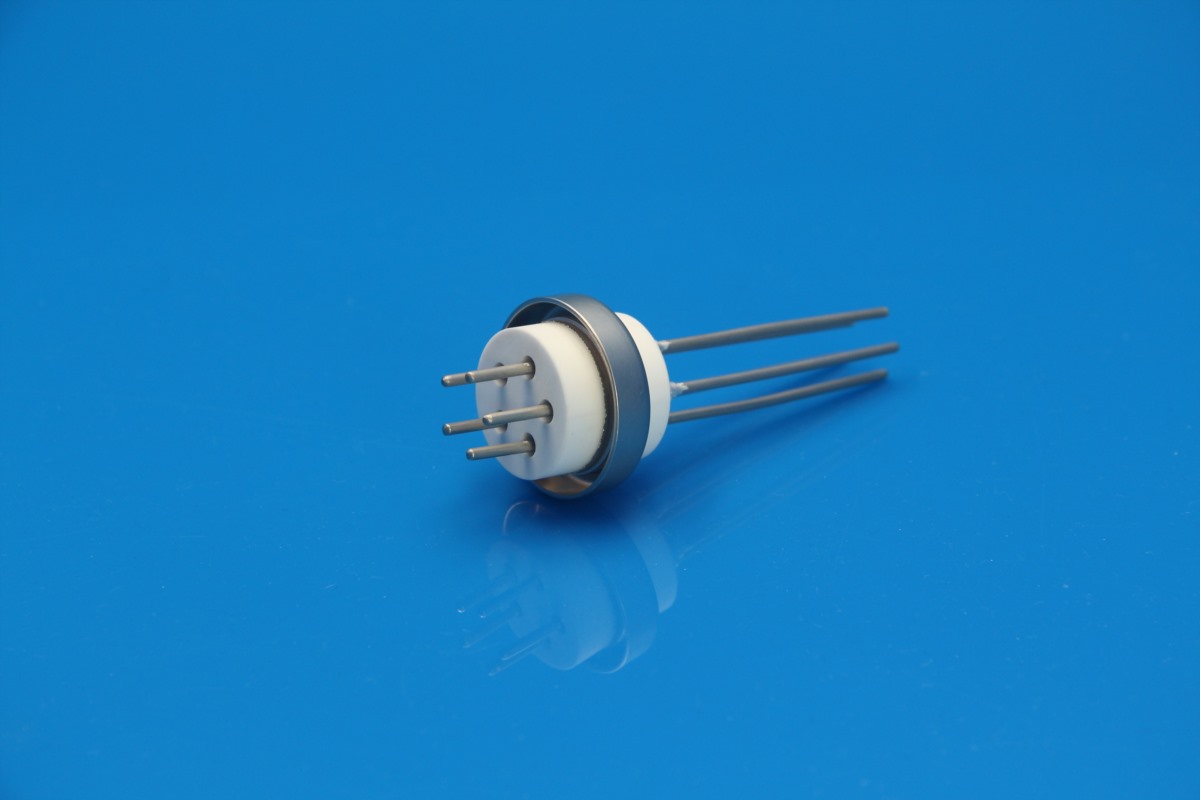
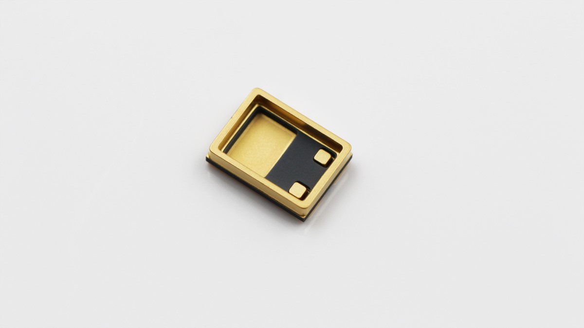
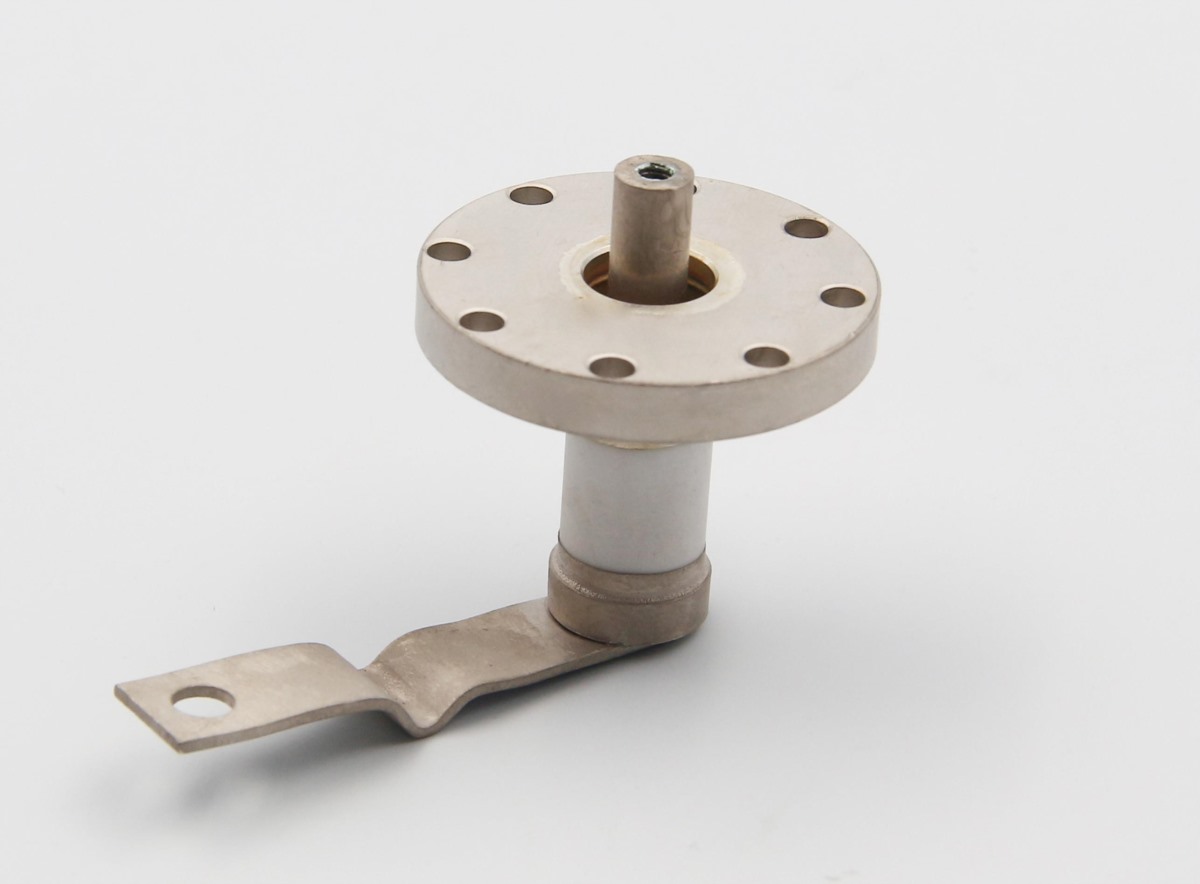
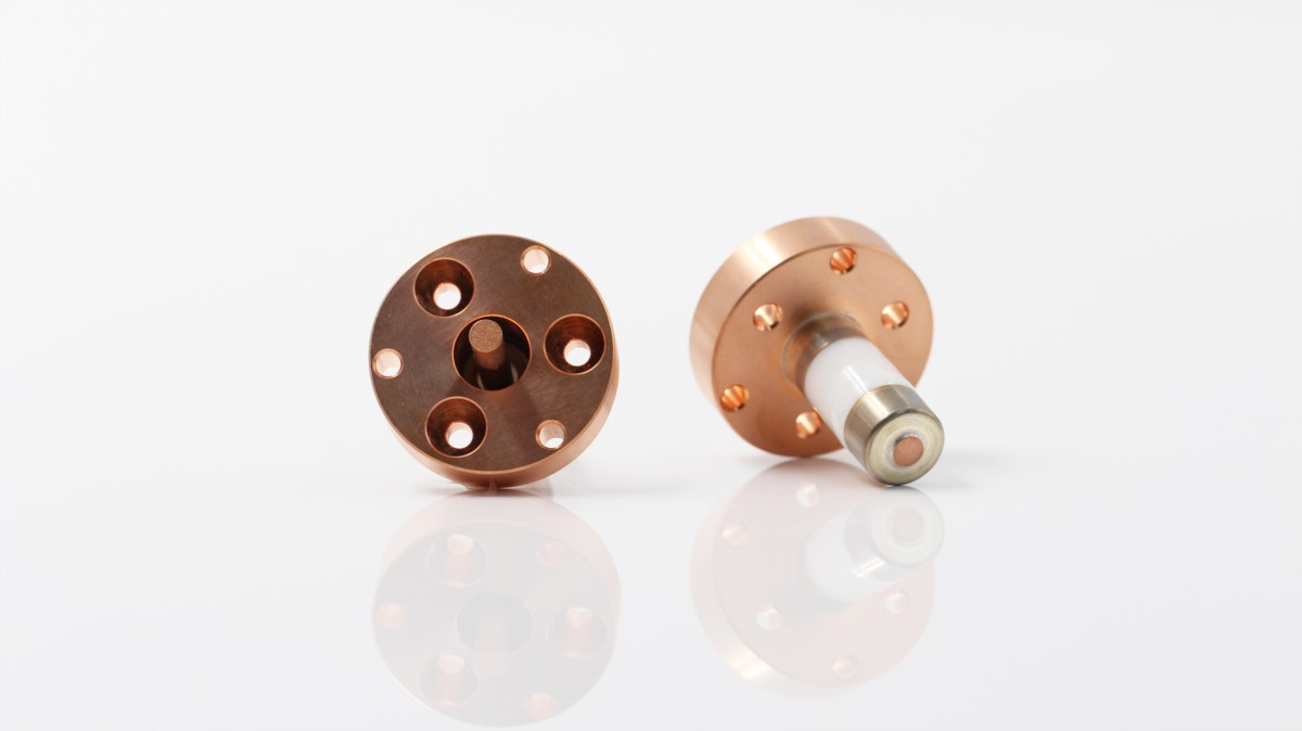
In response to this industry challenge, we have introduced the Ceramic Vacuum Feedthrough, manufactured using a mature high-temperature vacuum brazing process. Through the mature high-temperature vacuum brazing process, it achieves a permanent airtight connection between ceramics and metals, specifically designed for the demanding vacuum pressure environment.
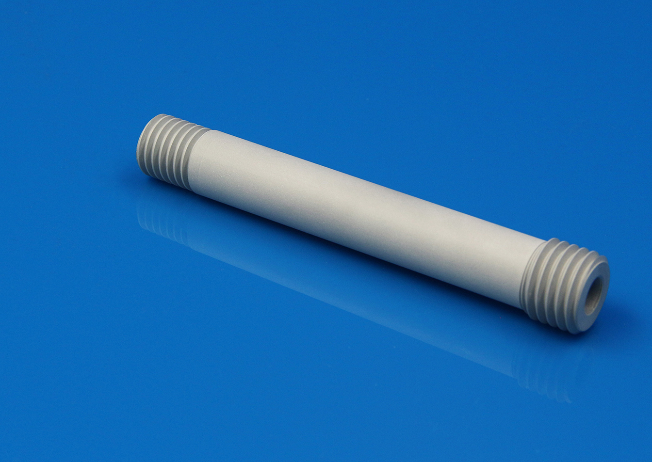
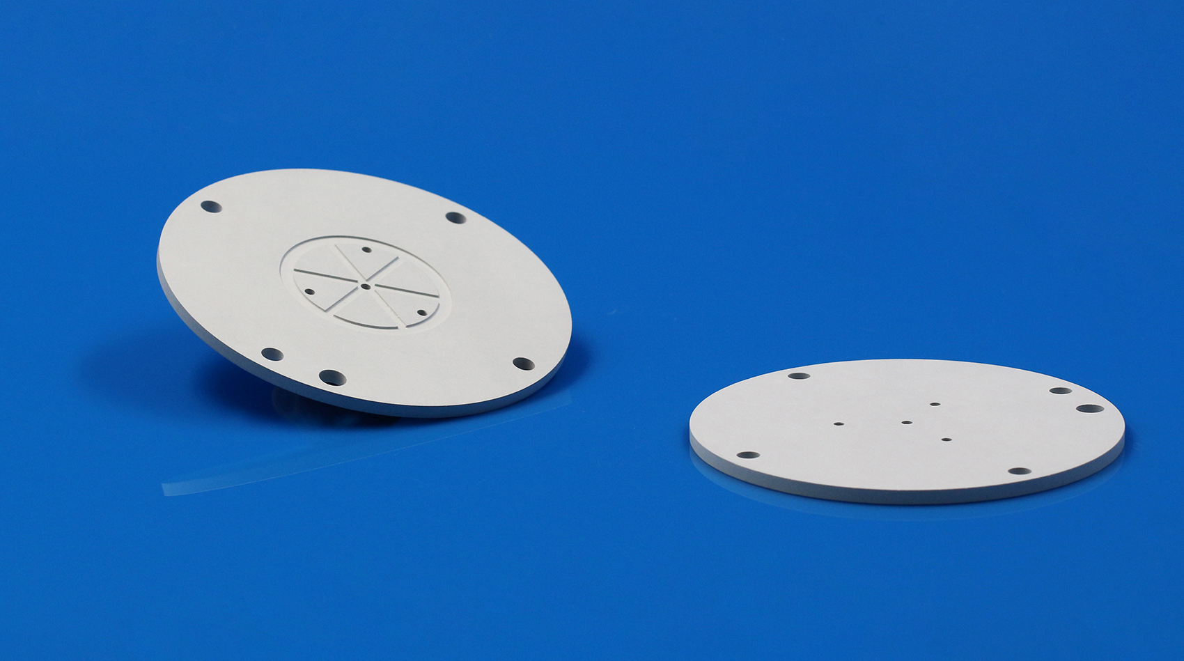
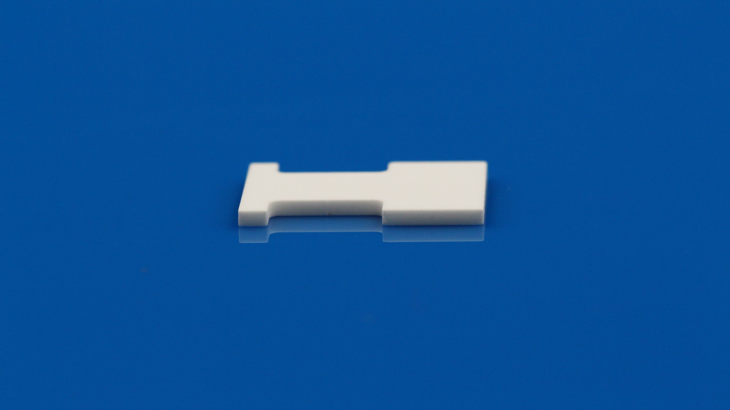
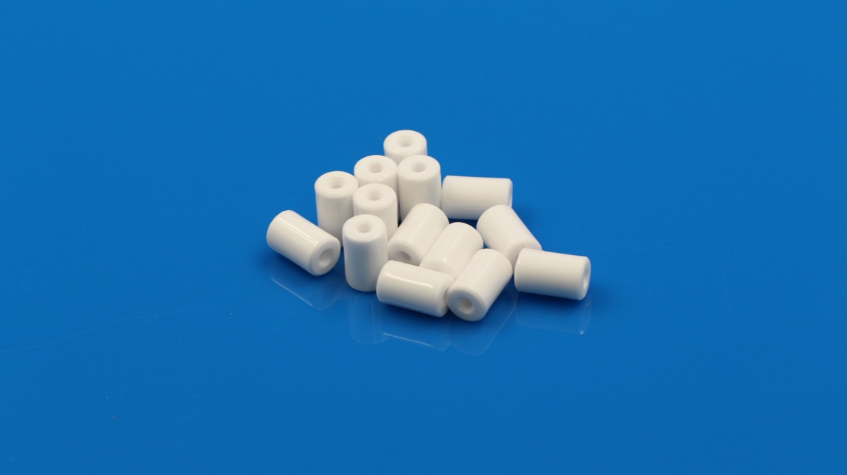
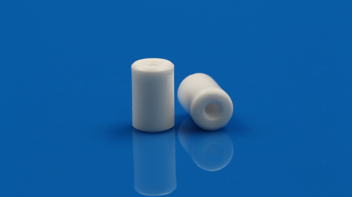
Structural Design Based on Engineering Requirements This component uses high-purity alumina ceramic as the insulating core, combined with metal materials (such as stainless steel, molybdenum or Kovar alloy) whose thermal expansion coefficient matches that of the ceramic. The high-temperature brazing is completed in a vacuum environment.
Key Process Advantages
– Vacuum brazing seal Employing a fully metal-ceramic sealed structure without any organic materials, this design avoids the problem of gas release during operation.
– High air-tight reliability The typical leakage rate can reach ≤ 10⁻⁹ mbar·L/s, meeting the requirements of high vacuum and ultra-high vacuum systems.
– High Temperature Resistance and Thermal Cycling Suitable for frequent start-stop and temperature-changing working conditions, with long-term stable sealing interface
– High insulation and low crosstalk The ceramic body has high dielectric strength and is suitable for the electrical connection requirements in precision analysis equipment.
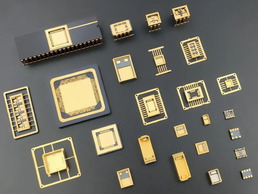
In semiconductor vacuum devices, electron microscopes, vacuum ovens and other equipment, Ceramic Vacuum Feedthroughs are widely used for the electrical connection of ion sources, electrodes or heating units. Compared with the traditional structure, its advantages lie in:
– Reduce the risk of system leakage
– Enhance the long-term operational stability of the entire machine
– Decrease the frequency of maintenance and replacement
– Support higher working temperatures and more demanding working conditions
Through continuous optimization in material selection and process control, this brazed ceramic vacuum welding component provides engineers with a predictable, verifiable and long-term applicable vacuum sealing solution, suitable for the design of vacuum systems with extremely high reliability requirements.

 Enquiry