Choosing the Right Ceramic Substrate for High-Power LED Thermal Management
In the context of the rapid popularization of LED lighting, thermal management has become a crucial factor determining the performance, reliability, and lifespan of LEDs. As LED technology advances towards higher power, higher brightness, and greater integration, the heat density per unit area continues to rise. Insufficient heat dissipation capacity will directly restrict the further improvement of device performance.
When the junction temperature is too high, LEDs will experience problems such as wavelength drift of light emission, attenuation of light efficiency, accelerated aging of phosphor, and a significant reduction in service life. Therefore, how to efficiently and stably transfer the heat generated by the chips has become a key issue in the design of high-power LED packages.
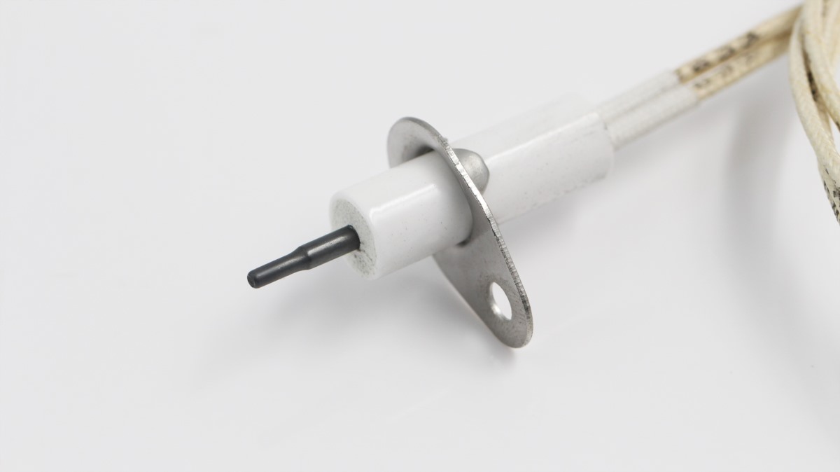
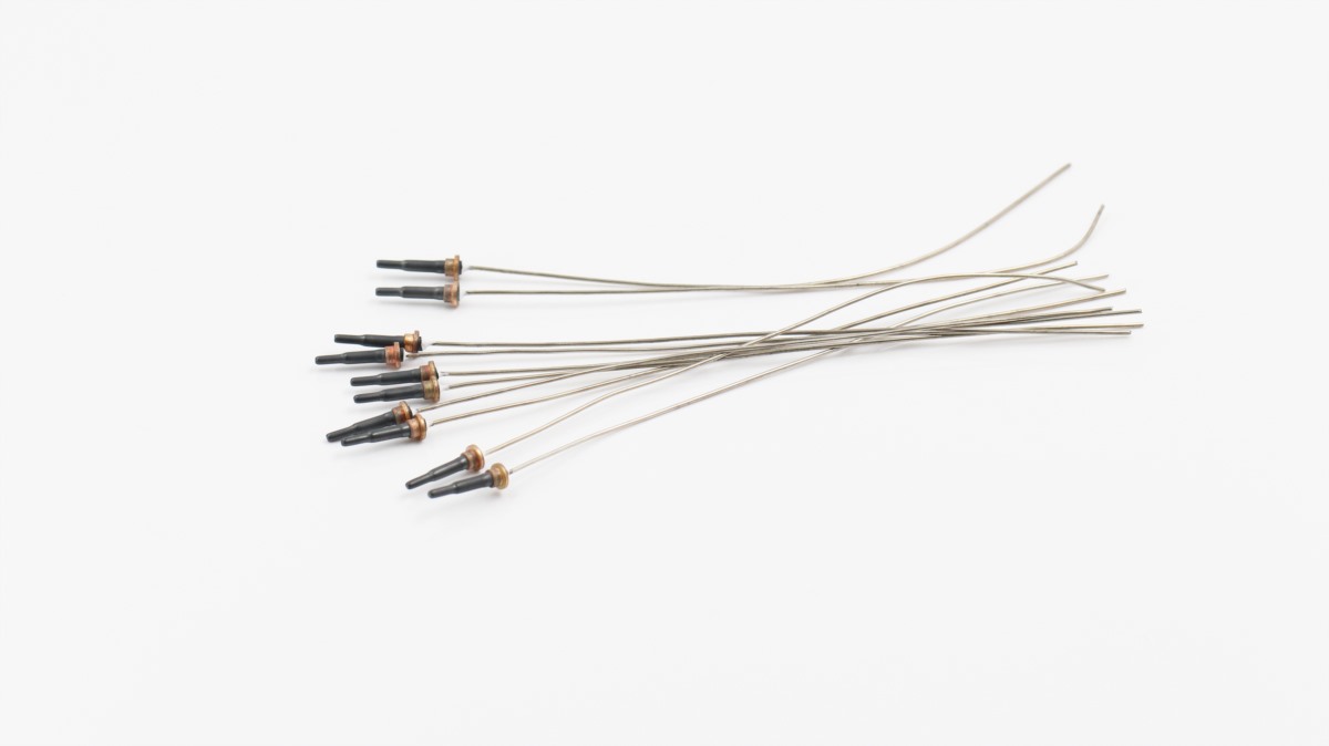
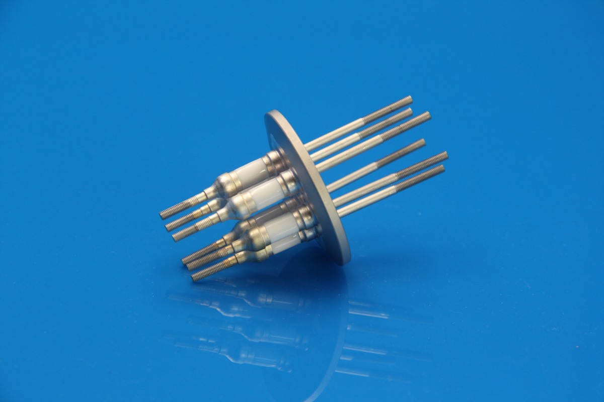
In reality, the heat generated by LED electronic devices is generally dissipated outward through the substrate. The substrate, as the core of thermal management, can quickly absorb the heat generated by the chip and achieve uniform heat distribution. Subsequently, it efficiently disperses the heat to the environment through the heat sink, ensuring the long-term stable operation of the LED.
The thermal conductivity, thermal resistance characteristics of the substrate, as well as its compatibility with the packaging process, directly determine the overall thermal management level of the LED. The ceramic substrate materials have performed quite well in these aspects and have gradually replaced the traditional metal or composite substrate materials to become the choice for high-power LEDs.
Ceramic substrate materials vary in performance and cost, and should be selected based on LED power level, thermal requirements, and application conditions.
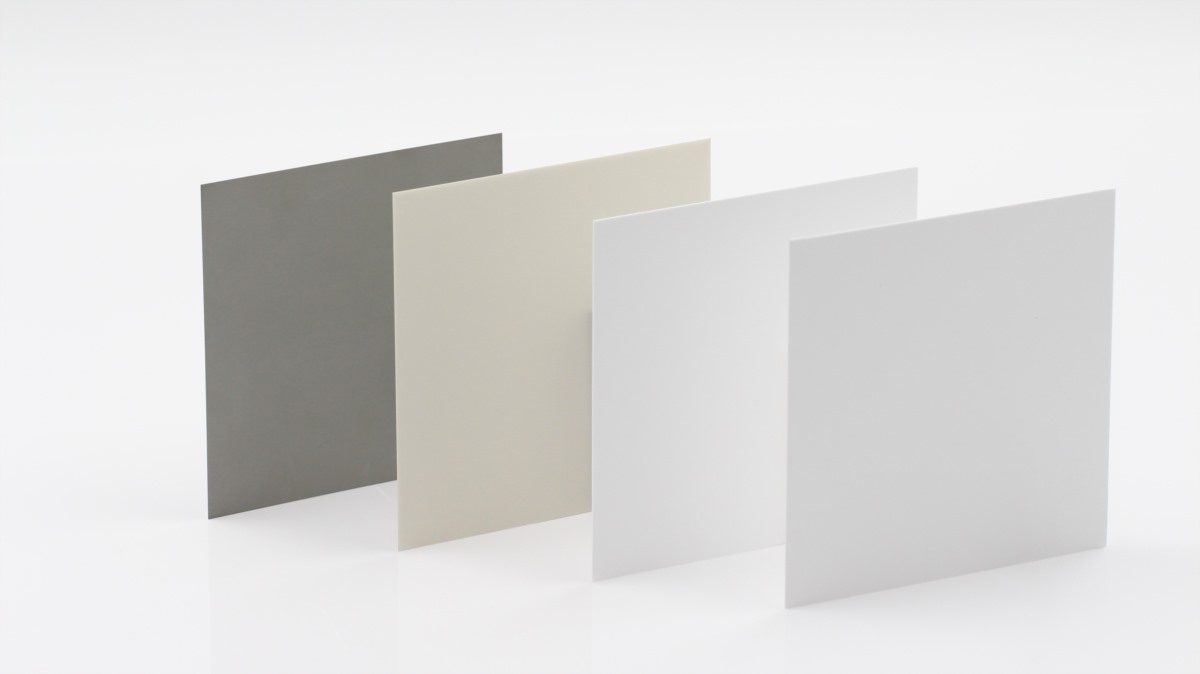
Common Ceramic Substrate Materials and Their Characteristics
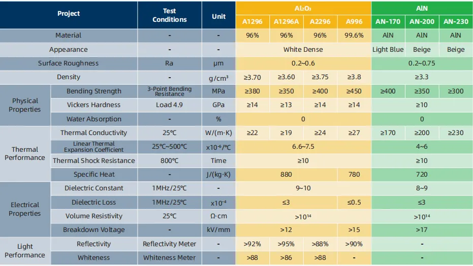
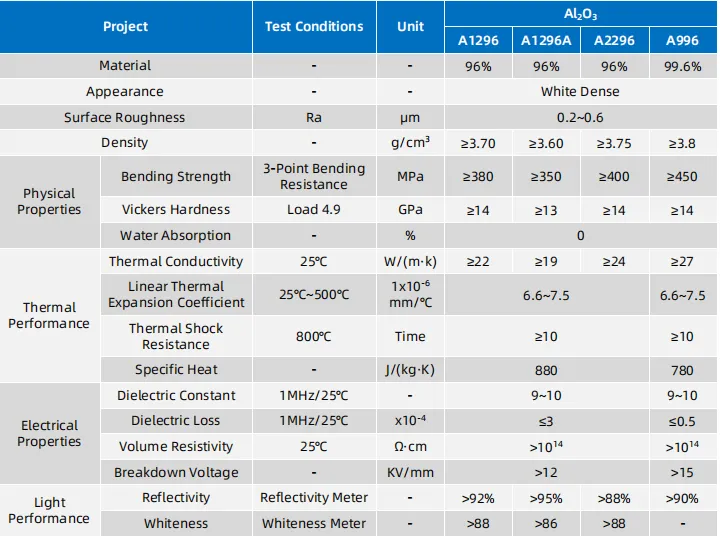
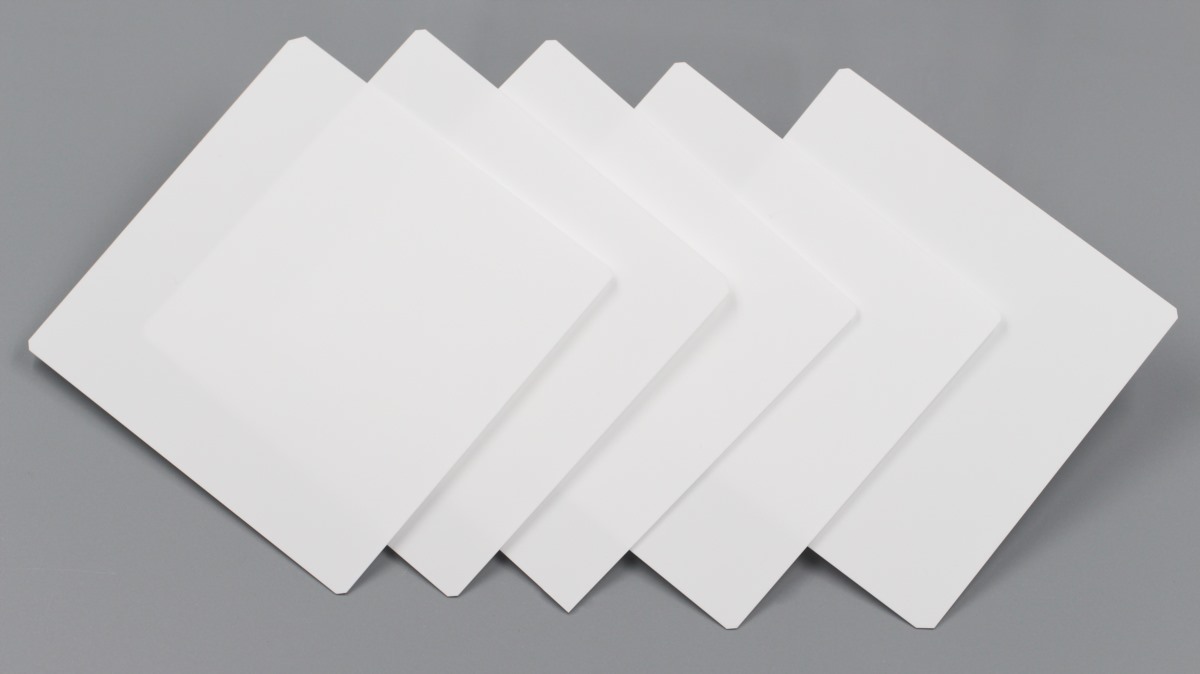
Alumina Substrate (Al2O3)
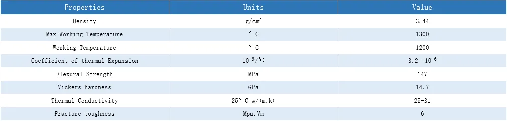
The most widely used ceramic substrate material at present. It has comprehensive advantages such as low cost, high mechanical strength, mature technology, and good reliability. Its thermal conductivity is typically between 20 and 30 W/m·K, which is sufficient to meet the heat dissipation requirements of medium and low-power LEDs. Therefore, it is a very cost-effective and practical choice in general lighting and applications where cost is a major concern.
Aluminum Nitride Substrate (AlN)
AlN offers 170–230 W/m·K thermal conductivity, far exceeding alumina. Its thermal expansion closely matches silicon chips, reducing thermal stress and improving reliability. With a low dielectric constant and excellent insulation, AlN is ideal for high-power, high-density LEDs and high-frequency devices.
Zirconia Toughened Alumina Substrate (ZTA)
ZTA is a composite ceramic made by adding zirconia to alumina. It offers high mechanical strength, excellent fracture toughness, and good reliability. Its thermal conductivity is higher than standard alumina but lower than AlN. ZTA is suitable for LED applications requiring high mechanical strength and thermal shock resistance, maintaining effective heat dissipation while enhancing crack resistance and long-term stability.
Silicon Nitride Substrate (Si₃N₄)
Si₃N₄ substrates offer high mechanical strength, excellent thermal shock resistance, and good thermal conductivity. They remain stable under large temperature variations and frequent thermal cycling, ensuring long-term reliability. Despite higher processing difficulty, Si₃N₄ is the preferred choice for LED and industrial applications demanding maximum reliability.
Key Factors for Selecting Ceramic Substrates
– Thermal conductivity: Controls junction temperature and heat efficiency.
– CTE matching: Reduces thermal stress for reliable operation.
– Dielectric/insulation: Ensures electrical safety and stable signals.
– Mechanical strength and processability: Suitable for packaging processes and long-term usage requirements.
– Cost and Customization: Meeting the requirements of various application scenarios and production scales.
Suggestions for Substrate Selection for LEDs of Different Power Ratings
1. Medium-Low Power LEDs (≤ 1 W)
The heat generation is relatively low, and the requirement for heat dissipation is relatively relaxed. The alumina (Al2O3) ceramic substrate can meet the temperature control requirements, featuring low cost and mature technology, and is suitable for general lighting and cost-sensitive applications.
2. Medium-Power LED (1–3 W)
The increase in heat density leads to higher demands for thermal conductivity and reliability. High-purity alumina or ZTA substrates, while balancing heat dissipation performance and mechanical strength, maintain a good cost-performance ratio and are suitable for conventional medium-power lighting applications.
3. High-Power LED (≥ 3 W)
Temperature control becomes the key. Aluminum nitride (AlN) ceramic substrates, with their high thermal conductivity and excellent thermal expansion matching, can effectively reduce the package thermal resistance and are the mainstream choice for high-power LEDs.
4. High Power Density and High Reliability Applications
Under conditions of high temperature, high stress, or frequent thermal cycling, silicon nitride (Si₃N₄) substrates, with their excellent mechanical strength and thermal shock resistance, are suitable for applications with extremely high reliability requirements.
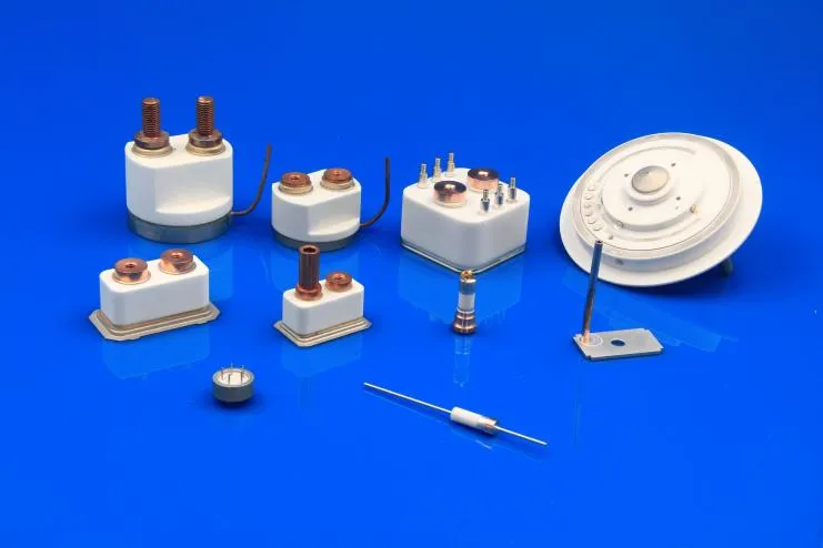
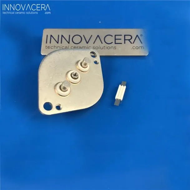
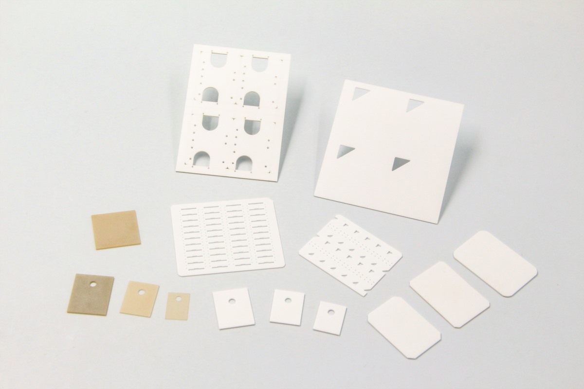
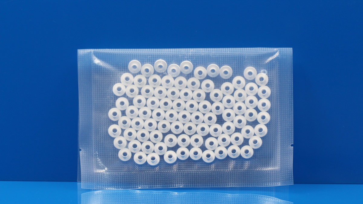
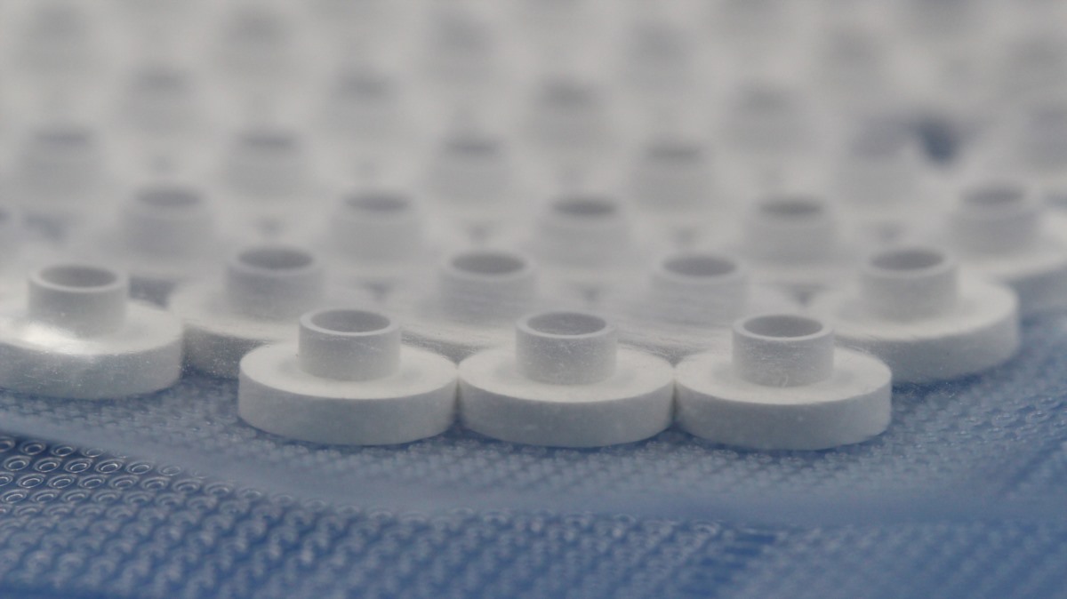
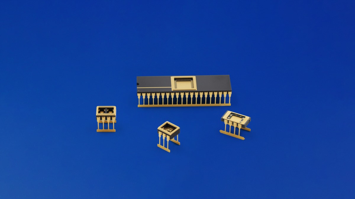
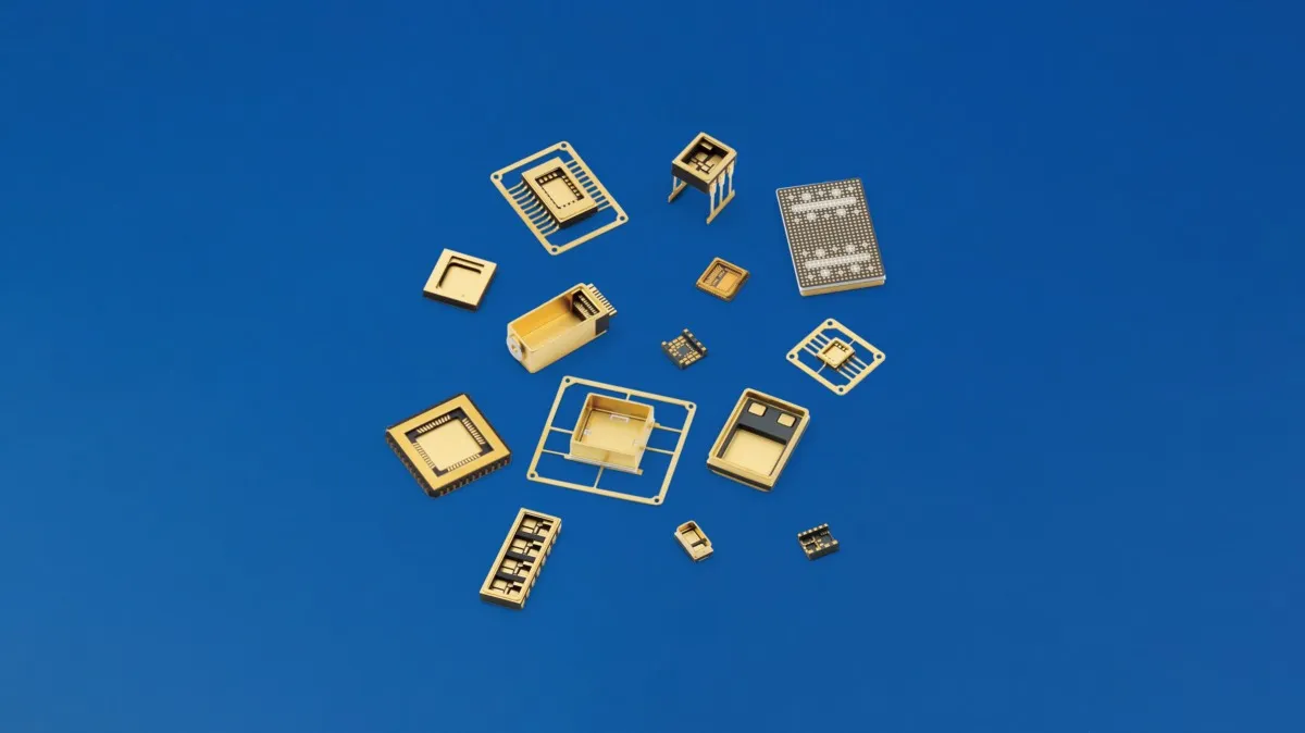
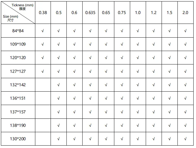
At Innovacera, we offer a variety of ceramic substrate materials and customized size solutions to meet the thermal management requirements of LEDs of different power levels.
 Enquiry