Ceramic substrates usually lead engineers to zero in on thermal conductivity, CTE, and dielectric strength right out of the gate. No surprise there—those are headline specs. But there’s a quieter parameter that tends to fly under the radar, and it can trip up an otherwise solid design. That parameter is surface roughness.
The real challenge? Thin-film and thick-film processes sit on opposite ends of the spectrum when it comes to what they need from a surface. Pick a finish that suits one, and you could be courting trouble for the other.
Thin-Film: Smooth Surfaces Win
Photolithography and precise deposition define thin-film fabrication. Even minor surface irregularities can distort line resolution or compromise via reliability. The margin for error here is slim.
For most standard applications, ground 96% or 99.6% alumina at Ra 0.2–0.6 μm fits the bill. ZTA comes in a touch flatter at 0.2–0.5 μm. AlN and Si₃N₄ typically arrive at 0.2–0.75 μm.
As geometries tighten and line widths shrink, polishing moves from optional to essential. Available finishes are summarized below:
| Process | Surface Roughness (Ra) |
|---|---|
| Grinding | 0.3–0.6 μm |
| Fine Grinding | 0.1–0.4 μm |
| Polishing (standard) | ≤ 0.1 μm |
| Polishing (special grade) | ≤ 0.05 μm |
At these smoother grades, fine-pitch designs become achievable. AlN and Si₃N₄ can be refined further when needed.
Thick-Film: A Bit of Grit Goes a Long Way
This one often raises eyebrows. Thick-film processing—screen-printing pastes and firing—actually has little use for a polished surface. Too smooth can even backfire.
Consider how the bond works. Chemical attraction does part of the job, but surface texture adds a mechanical component: the paste seeps into microscopic peaks and valleys, creating a physical lock. That extra hold becomes critical when the part endures heat cycles or mechanical vibration. Remove that texture, and you lose a layer of durability.
That’s precisely why the standard as-fired or ground finishes suit thick-film work so well:
| Material | Standard Ra Range |
|---|---|
| 96% / 99.6% Al₂O₃ | 0.2–0.6 μm |
| ZTA | 0.2–0.5 μm |
| AlN | 0.2–0.75 μm |
| Si₃N₄ | 0.2–0.75 μm |
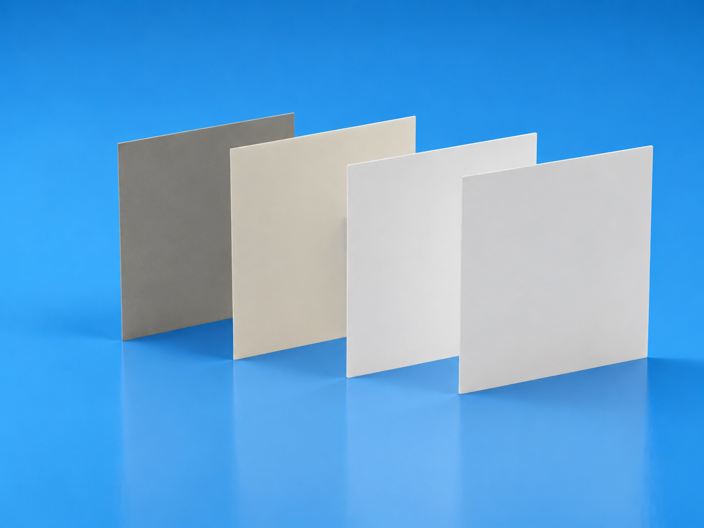
Here, roughness isn’t a defect—it’s a contributor to performance.
Which Way to Go?
Each project brings its own set of requirements. For thin-film, the goal is flat and finer—polished surfaces below 0.1 μm are standard once feature sizes shrink. For thick-film, resist the urge to over-polish. The conventional ground finish (0.2–0.6 μm) already gives the paste the texture it needs. Going smoother could weaken the bond rather than strengthen it.
Suppliers typically carry multiple finishing tiers—grinding, fine grinding, polishing—so you’re not locked into one option. Choosing the right one upfront saves headaches later on, when parts are already in production rather than still on paper.