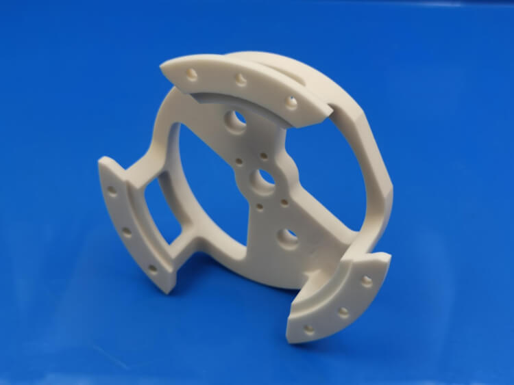
Alumina Ceramic parts are used for rotating parts in photolithography machines and in a vacuum state. This requires extremely high machining accuracy, and the runout of the inner circle is required to be within 2 microns.
Fine ceramics have become key components of semiconductor equipment. Especially in high-end lithography machines, in order to achieve high process accuracy, it is necessary to widely use ceramic components with good functional composite, structural stability, thermal stability, and high dimensional accuracy.Such as E-chuck, Vacumm-chuck, Block, magnetic steel skeleton water-cooled plate, reflector, guide rail, etc.

Alumina ceramic parts for photolithography machines
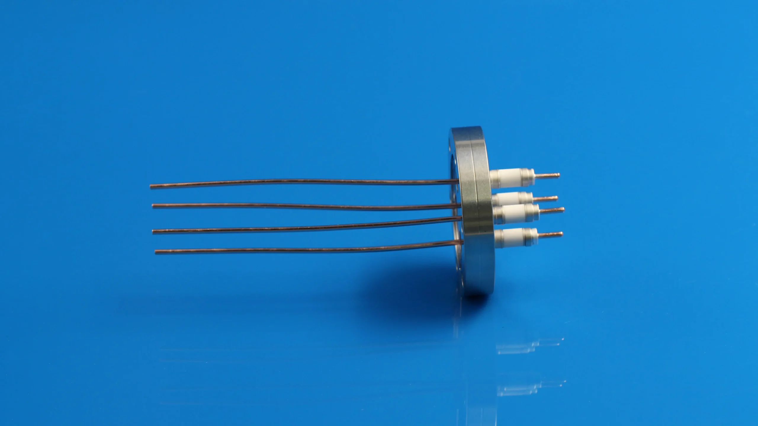
Another high precision ceramic parts used in the semiconductor industry Precision ceramics have become key components of semiconductor equipment, including single crystal furnaces, ion implantation equipment, photolithography machines, CVD/PVD equipment, and packaging and testing equipment.
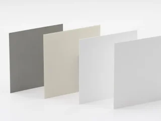
Innovacera can provide the required materials including alumina ceramics, aluminum nitride ceramics, silicon nitride ceramics, boron nitride//pyrolytic boron nitride ceramics, silicon carbide and microporous ceramics.
Fine Ceramic used in semiconductor industry
Declaration: This is an original article of INNOVACERA®. Please indicate the source link when reprinting: https://www.innovacera.com/news/alumina-ceramic-parts-as-photolithography-machines-in-the-semiconductor-industry.html.


 Enquiry