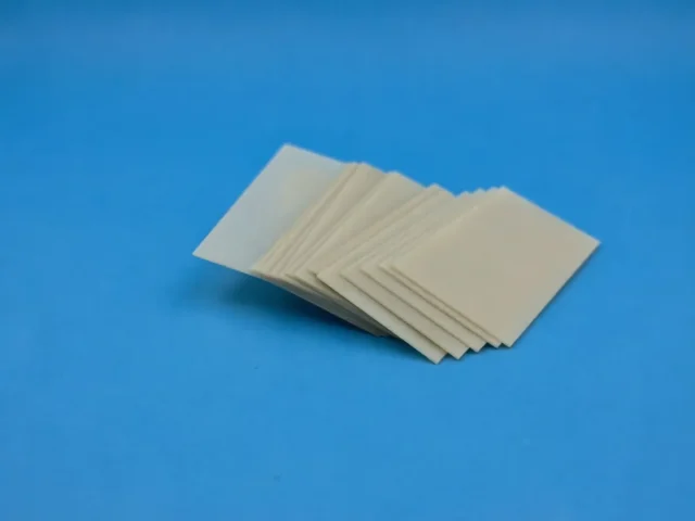
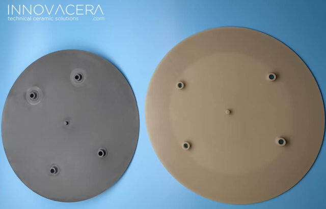
If you work in DPC, thick film, thin film, or DBC ceramic circuits, you already know this: not all ceramic substrates are created equal. And when it comes to aluminum nitride (AlN), the gap between “good enough” and “truly qualified” can make or break your metallization yield.
Let me walk you through what actually matters when you’re qualifying AlN bare substrates for DPC processing—and why getting this right saves you headaches down the line.

Why AlN for DPC?
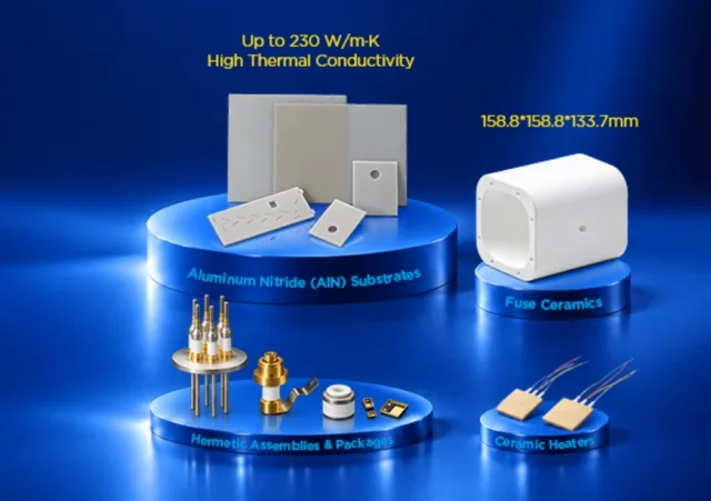
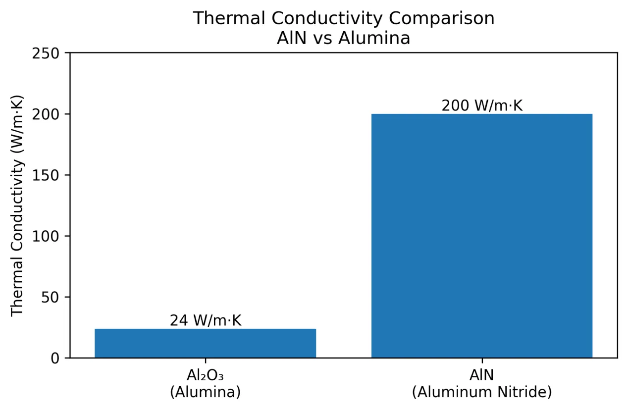
AlN is the material of choice for DPC metallization for one simple reason: it moves heat. Its thermal conductivity sits in the range of 170 to 230 W/m·K—roughly seven to ten times that of alumina. That kind of performance is what lets high-power devices actually survive in the field. On top of that, its coefficient of thermal expansion (about 4.5 ppm/K) closely matches silicon and silicon carbide, so you don’t get delamination or solder joint fatigue when things heat up and cool down.
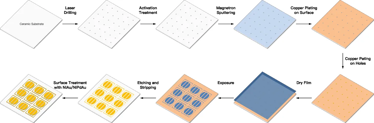
DPC itself is a thin-film metallization process that starts with sputtering a metal layer—typically titanium as an adhesion layer followed by copper—onto the ceramic surface. Then comes photolithography, plating, and etching to create fine circuit patterns. The result? High-precision traces with line widths down to 20–30 microns and surface flatness under 0.3 microns. That’s the kind of precision you need for today’s compact, high-density modules.
What to Look For When Qualifying AlN Substrates?
Here’s where things get practical. You’re not just buying a sheet of ceramic—you’re buying a foundation for your entire metallization process. And the foundation has to be right.
Surface quality is the first thing to check. DPC relies on vacuum sputtering to deposit the initial metal layer. If your substrate surface has scratches, pits, or contamination, the adhesion layer won’t bond properly. One rule of thumb I’ve learned over the years: surface roughness should be controlled to Ra < 0.3μm for good mechanical interlocking with the metallization layer. Go too rough, and you trap plating solution residues. Go too smooth, and you lose mechanical grip. It’s a balancing act.
Flatness and warpage matter more than you might think. DPC involves multiple high-temperature steps—sputtering, annealing, plating. If the substrate bows or twists, your photolithography alignment goes out the window. Consistent thickness and minimal warpage are non-negotiable.
Purity drives thermal performance. High-purity AlN (above 99%) delivers thermal conductivity that can exceed 200 W/m·K. But impurities—especially oxygen—create phonon scattering that drags that number down. So when you’re qualifying a supplier, ask for the purity data and the actual tested thermal conductivity, not just the “typical” spec sheet numbers.
Laser drillability is another practical concern. DPC often requires vias for vertical interconnection, typically drilled by laser with diameters from 60 to 120 microns. The substrate needs to laser-cleanly without micro-cracking or excessive taper. That comes down to material consistency—grain size, density, and absence of internal defects.
How We Approach This
We don’t just ship AlN substrates and hope they work in your process. We start by understanding your specific DPC line—your sputtering parameters, your plating chemistry, your thermal profiles. Then we recommend substrates that are actually compatible, not just “close enough.”
Our materials research team can adjust formulations to hit your target thermal conductivity, surface finish, and mechanical properties. If you need a particular surface roughness for better adhesion, we can dial it in. If you’re running into via drilling issues, we can look at grain structure and density. We’ve been down this road with enough customers to know that the “standard” solution rarely fits everyone.
And if something doesn’t work? We don’t point fingers. We dig in, run failure analysis, and figure out whether it’s a substrate issue, a process issue, or something in between. Then we fix it.
The Bottom Line
Qualifying AlN substrates for DPC metallization isn’t complicated—but it does require attention to the right details: surface quality, flatness, purity, and consistency. Get those right, and your metallization yield climbs. Get them wrong, and you’ll spend weeks chasing adhesion failures and alignment errors.
If you’re running into technical challenges with ceramic substrates—whether it’s thermal performance, metal adhesion, via formation, or anything else—we’re here to help. Our engineering team has worked with DPC process engineers across the board, and we genuinely enjoy solving the tricky ones. Drop us a line. We’ll listen, we’ll propose, and we’ll work alongside you until you have a solution that actually runs on your production floor.