From CPO and External Laser Sources to AlN Ceramic Thermal Packaging
AI clusters are driving optical links toward higher bandwidth, higher optical power and tighter integration. As optical engines move closer to high-power switch ASICs, thermal management is no longer only a rack- or system-level cooling problem. It is increasingly a packaging and materials problem.
- Higher heat density around optical engines and switch silicon
- Shorter thermal paths between electronics and photonics
- More temperature-sensitive lasers operating at higher optical power
1. Why AI Optical Interconnects Are Getting Hotter
AI scale-up and scale-out networks move enormous amounts of data between accelerators, switches and racks. Electrical interconnects become increasingly difficult to scale because higher data rates raise power consumption and signal-integrity challenges. Optical interconnect therefore moves closer to the switch ASIC, reducing electrical reach but increasing the thermal interaction between photonic and electronic devices.
The key change is not simply that an AI data center consumes more power. The heat is becoming concentrated in smaller packages, while optical components must maintain stable wavelength, output power and signal quality.
2. From Pluggable Optics to CPO: Shorter Electrical Paths, Higher Thermal Coupling
| Architecture | Typical electrical relationship | Thermal coupling |
|---|---|---|
| Pluggable / LPO | Optical module remains at the front panel | Lower |
| NPO | Optical engine moves closer to the switch ASIC | Higher |
| CPO | Optical engine is packaged adjacent to the switch ASIC | High |
As electrical distance decreases, thermal coupling between electronics and photonics increases. This is one of the central thermal-management consequences of the transition toward NPO and CPO.
3. Why Temperature Matters to Lasers and Photonics
Semiconductor lasers are temperature-sensitive devices. Higher junction temperature can reduce slope efficiency, change wavelength, increase threshold current and accelerate degradation. For high-power CW DFB lasers, the relevant question is therefore not only ambient temperature, but how efficiently heat can move from the laser junction into the package.
A simplified thermal path is:
Laser Junction → Laser Die → Die Attach → Ceramic Submount → Package / TEC → Heat Sink
Every interface contributes thermal resistance. As optical power rises, small improvements in the die-attach layer, submount material, flatness and interface quality can have a meaningful effect on junction temperature.
4. Why External Laser Sources Are Emerging
CPO places the optical engine very close to high-power switching silicon. Keeping a high-power laser inside this thermally dense region can complicate temperature control, serviceability and long-term reliability. One response is to separate the continuous-wave laser from the optical engine and deliver light through fiber.
This external-laser approach also supports field replaceability: a laser source can be serviced independently rather than requiring replacement of a costly co-packaged switch-and-optics assembly. Industry activity around external laser source form factors reflects this architectural shift.
5. High-Power CW Lasers Change the Packaging Problem
Once the CW DFB laser becomes an independent source for multiple optical channels, required output power can move from tens of milliwatts toward hundreds of milliwatts per channel or source. At these power levels, laser packaging is no longer only an optical-alignment problem. It becomes a combined thermal, mechanical and electrical design problem.
- Low thermal resistance from laser die to package base
- Stable mechanical support and controlled coefficient of thermal expansion (CTE)
- Electrical insulation where required
- Metallizable surfaces for die attach, wire bonding or package integration
- Tight flatness and surface-finish control
6. Why AlN Ceramic Is Relevant
This is where high-thermal-conductivity, electrically insulating materials such as aluminum nitride (AlN) become important. The value of AlN is not a single property; it is the combination of thermal conductivity, electrical insulation, semiconductor-compatible thermal expansion and compatibility with metallization.
| Property | AlN | Al₂O₃ | Copper |
|---|---|---|---|
| Thermal conductivity | High | Moderate | Very high |
| Electrical insulation | Yes | Yes | No |
| CTE compatibility with semiconductor packaging | Good | Moderate | Limited |
| Metallization capability | Yes | Yes | N/A |
| Typical role | Laser submount / heat spreader | General insulating substrate | Metal heat spreader |
For optical packaging, this balance can make AlN suitable for laser submounts, heat spreaders and metallized carriers where heat must be removed while electrical isolation and dimensional stability are maintained.
7. Key Material Requirements for Laser Submounts
Material selection alone does not determine thermal performance. A laser submount must be evaluated as part of the complete thermal stack. Important engineering parameters include:
- Thermal conductivity and thickness
- Submount dimensions and heat-spreading area
- Flatness, parallelism and surface roughness
- Metallization system and pattern
- Die-attach method and interface thickness
- Operating and assembly temperatures
- CTE interaction with the laser die and package
8. Ceramic Components for High-Power Optical Packaging
Depending on the optical architecture and package design, ceramic components may include:
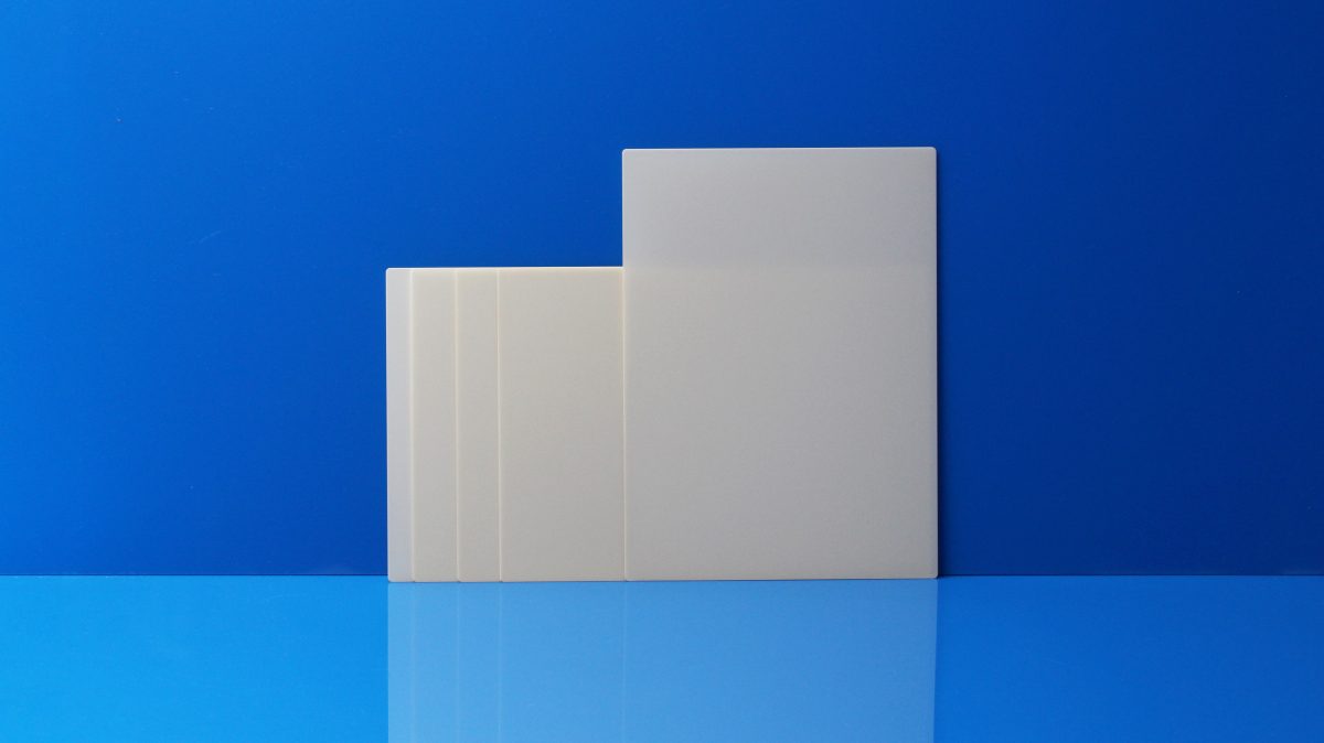
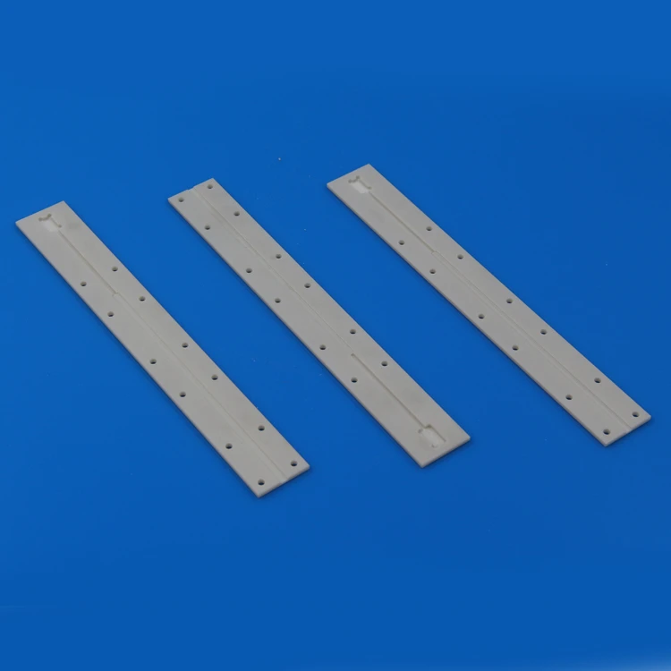
- AlN laser submounts
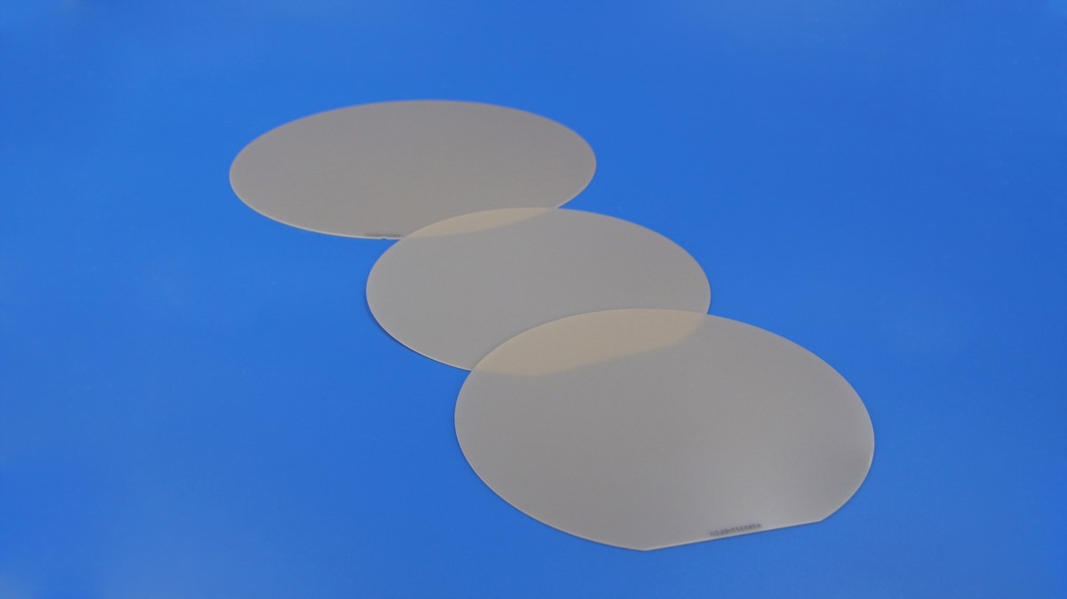
- Metallized AlN substrates
- AlN heat spreaders
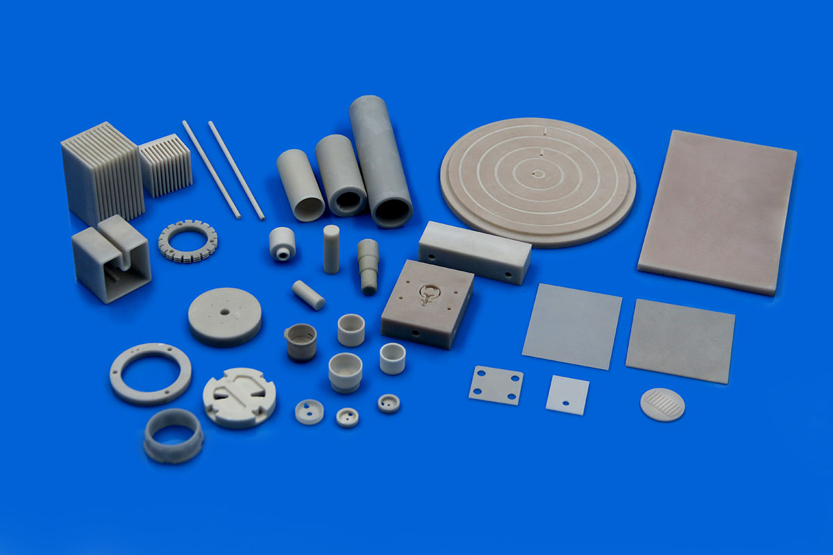
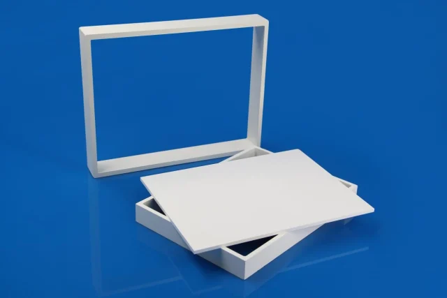
- Precision ceramic carriers
- Custom ceramic packaging components
For custom evaluation, the most useful starting information is material, dimensions, thickness, surface finish, flatness, metallization requirement, die-attach process and operating temperature.
9. Thermal Management Is Becoming Part of Optical Architecture
The evolution from pluggable optics to NPO and CPO shows that thermal design can no longer be treated as a downstream cooling task. Optical architecture, laser location, package design and material selection are becoming interdependent.
For high-power optical sources, the engineering question is increasingly: how can heat be moved away from the laser junction with the lowest practical thermal resistance while preserving electrical isolation, optical stability and package reliability?
10. From Optical Architecture to Ceramic Packaging
As AI optical interconnects scale toward higher bandwidth and denser integration, thermal-management decisions are moving closer to the device and material level. AlN ceramic is relevant because it can form part of the shortest thermal path between a high-power laser die and the cooling structure.
This makes laser submount design, metallization, surface quality and ceramic thermal performance increasingly important considerations in next-generation optical packaging.
Related topic: Why AlN Ceramic Is Becoming Important for High-Power CW DFB Laser Packaging.