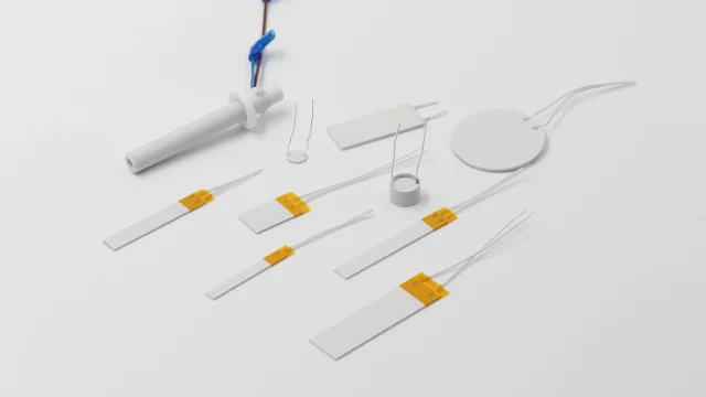
As semiconductor manufacturing processes develop toward higher precision and integration, equipment used for etching, thin-film deposition, plasma cleaning and other procedures is subject to rising demands for long-term stable operation.
Ceramic dielectric components installed in semiconductor plasma equipment work continuously in vacuum, high-temperature, high-frequency RF electric field and reactive plasma environments, and must meet multiple criteria simultaneously: electrical insulation performance, structural stability, corrosion resistance and accurate assembly.
While substrate materials do not take part in wafer processing directly, their material properties, machining precision and batch consistency will impact internal electric field distribution, plasma stability and chamber pollution control.
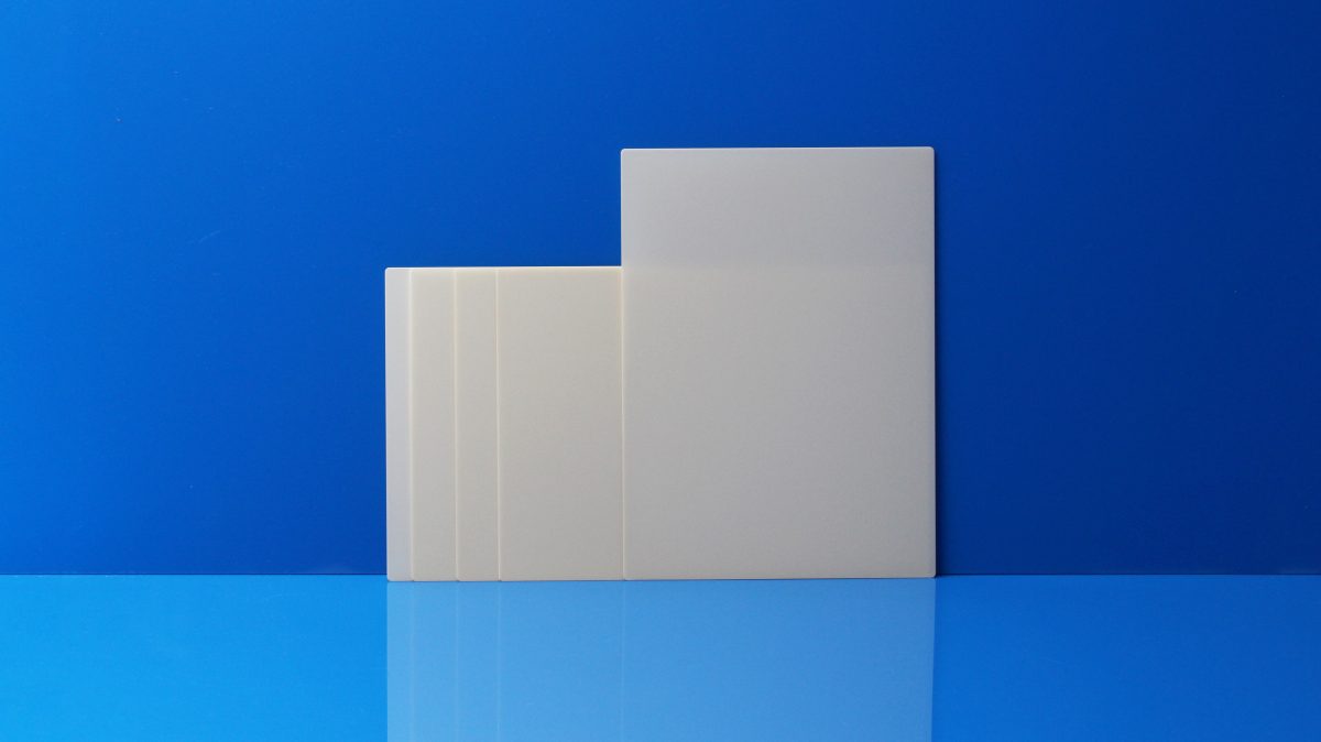
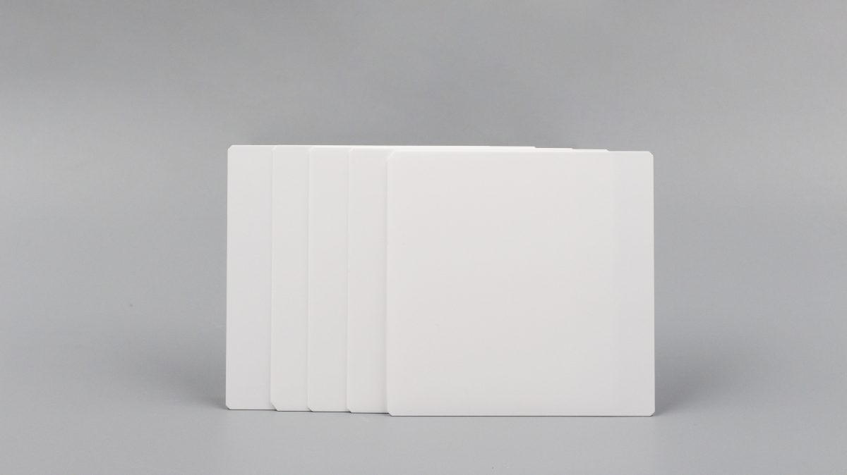
Thus, high-reliability alumina ceramic dielectric substrates are indispensable basic insulating components for semiconductor etching, deposition and vacuum equipment.
I. What challenges do dielectric substrates face in semiconductor plasma equipment?
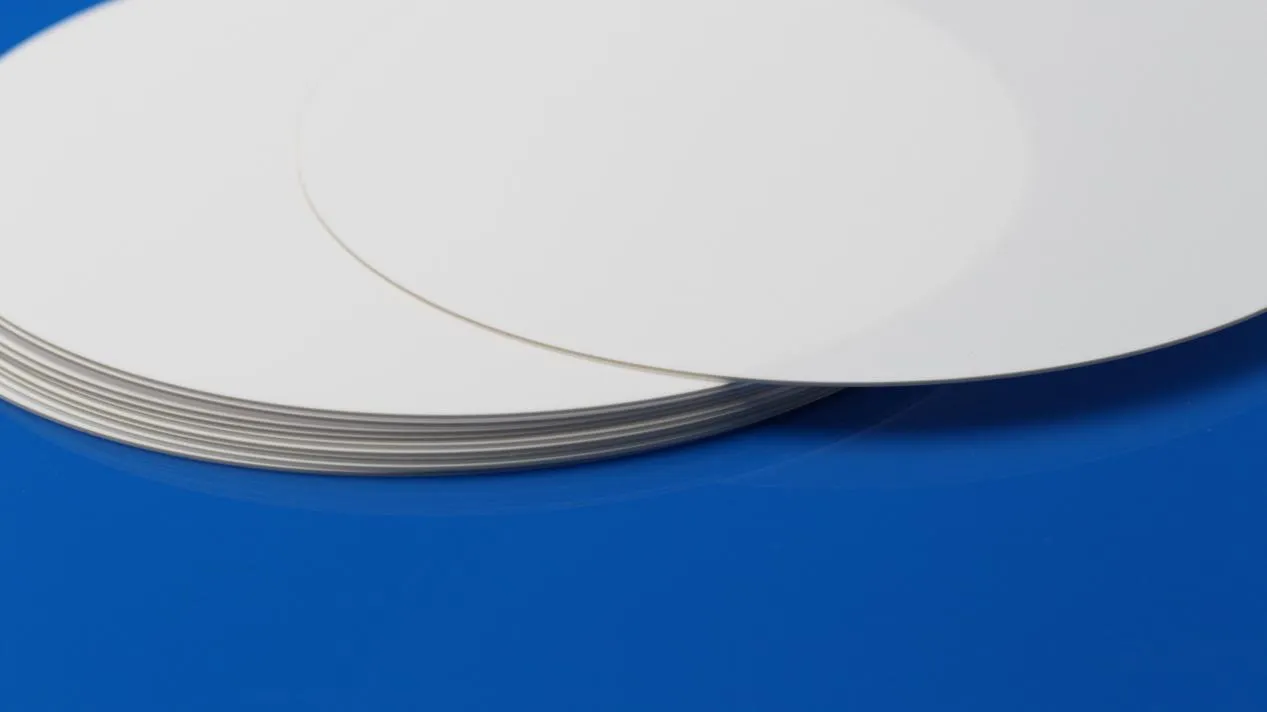
In etching, CVD, and PVD equipment, aluminum oxide ceramic dielectric substrates are commonly used in RF insulation structures, electrode isolation components, and vacuum chamber support parts.
Due to the complex working environment, the substrate must withstand prolonged exposure to combined electrical, thermal, and chemical conditions.
Therefore, alumina ceramic dielectric substrates for semiconductor equipment must not only meet basic material performance requirements, but also require attention to dimensional control, surface quality, and batch consistency.
II. Why Alumina Ceramic Is Suitable for Plasma Equipment Dielectric Materials
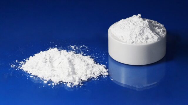
Alumina ceramic (Al2O3) is a highly mature engineering ceramic material widely adopted in semiconductor equipment. It features balanced and comprehensive performance rather than outstanding single indicators, delivering excellent integration of electrical insulation, mechanical strength, thermal stability and processing consistency.
1. Stable electrical insulation performance
Plasma equipment generates and regulates plasma via RF power supplies, so dielectric materials must sustain stable insulating performance over the long term to avoid malfunctions stemming from fluctuating electrical characteristics.
Alumina ceramics boast high volume resistivity and consistent dielectric properties, ideal for insulation and supporting structures within RF assemblies.
2. Excellent high-temperature dimensional stability
Semiconductor equipment chambers are subjected to prolonged high-temperature operating conditions, along with frequent start-ups and shutdowns that cause temperature fluctuations.
Alumina ceramics possess high mechanical strength and excellent thermal stability, reducing the risk of deformation and cracking during prolonged thermal cycling.
3. Resistance to plasma environment
In plasma environments based on fluorine, oxygen, and similar elements, equipment materials are subject to continuous erosion.
High-density alumina ceramics can reduce surface wear of the material and enhance long-term chamber operational stability by minimizing impurity release through controlled purity levels and processing quality.
III. How to choose among different grades of alumina purity?
The purity of alumina will affect the density of the material, the content of impurities, and its ability to withstand plasma environment. In practical equipment applications, the selection needs to be made based on process requirements, pollution control levels, and cost factors.
| Alumina Grade | Main Features | Typical Application Fields |
|---|---|---|
| 95% Al₂O₃ | Stable overall performance, prominent cost advantage, mature processing technology | General insulating structural parts, common industrial vacuum components |
| 96% Al₂O₃ | Balanced insulation performance, mechanical strength and machinability | Dielectric components for semiconductor equipment, RF insulating parts and other mainstream options |
| 99% Al₂O₃ & Above | Higher purity, superior impurity control capacity | Semiconductor equipment applications with strict requirements for particle control and material stability |
For semiconductor plasma equipment, the material grade is not necessarily the higher the better. Instead, it needs to be evaluated comprehensively based on the equipment structure, process environment, and reliability requirements.
IV. What parameters should be considered when purchasing alumina dielectric substrates for semiconductor equipment?
For equipment manufacturers and ceramic component purchasing enterprises, material purity is merely a basic requirement. What truly affects the long-term performance is also the processing accuracy and quality consistency.
| Key Parameter | Focus of Attention | Impact on Equipment Application |
|---|---|---|
| Alumina Purity | Al₂O₃ content and impurity control level | Affects corrosion resistance and contamination control |
| Overall Dimensions | Length, width, outer diameter and dimensional tolerances | Affects equipment assembly and matching accuracy |
| Thickness Tolerance | Single-piece thickness and batch consistency | Affects component assembly and electric field stability |
| Warpage / Flatness | Overall planar state | Affects fitting effect and structural stability |
| Surface Roughness | Ra value and surface uniformity | Affects subsequent processing, contamination control and bonding reliability |
| Edge Quality | Control of edge chipping and cracks | Reduces the risk of breakage during installation and operation |
| Batch Consistency | Performance fluctuation across different batches | Reduces risks in equipment commissioning and mass production |
For semiconductor equipment that operates over a long period, the performance of a single sample meeting the standards does not imply the ability to supply in a stable batch. The material control, precision processing capabilities, and quality inspection systems of the supplier are also important factors in the procurement assessment.
V. How to reduce the risk of substrate introduction in the alumina medium?
During the project development and supplier evaluation stages, it is not advisable to make selections solely based on material names or size specifications. Instead, technical requirements should be determined in conjunction with the actual equipment operating conditions.
During the inquiry or sample evaluation stage, the customer can provide:
• Sample size and structure drawings;
• Requirements for alumina purity grade;
• Thickness and size tolerance requirements;
• Surface roughness and flatness standards;
• Working temperature and vacuum environment;
• RF application conditions;
• Subsequent assembly or processing requirements.
By matching the material grades with the processing parameters in advance, the sample verification cycle can be shortened and the stability of the equipment during the mass production stage can be enhanced.
VI. Innovacera Alumina Ceramic Dielectric Substrate Solution
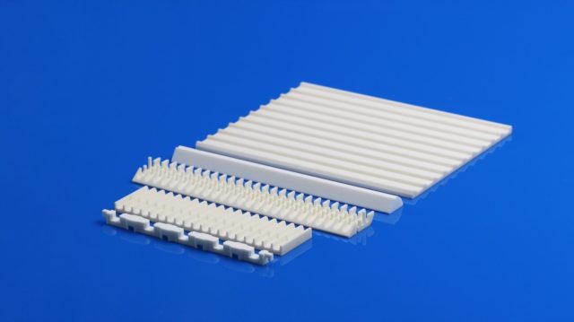
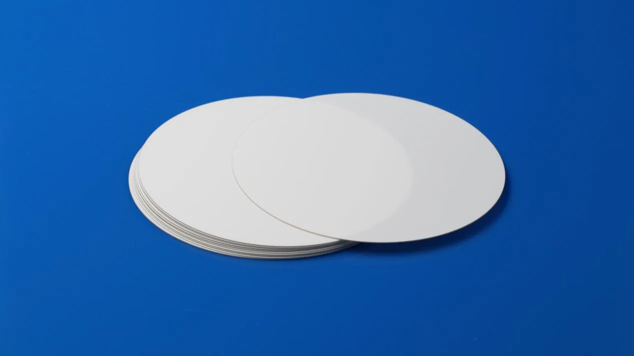
Innovacera can provide alumina ceramic substrate for semiconductor plasma equipment and precise insulating ceramic components, supporting customization of circular, square and irregular shapes.
The products cover different purity grades of alumina materials such as 95%, 96%, and 99%. They can be customized according to application requirements:
• Customized size and thickness processing;
• Precision grinding and surface control;
• Optimization of surface roughness;
• Batch consistency control.
The product can be applied to semiconductor etching equipment, thin film deposition equipment, vacuum equipment and other high-reliability insulating structures.
If you need to evaluate the alumina ceramic dielectric substrate solution, please provide the product size, working environment and processing requirements. Innovacera will offer a matching ceramic solution based on the specific application needs. Please contact sales@innovacera.com.