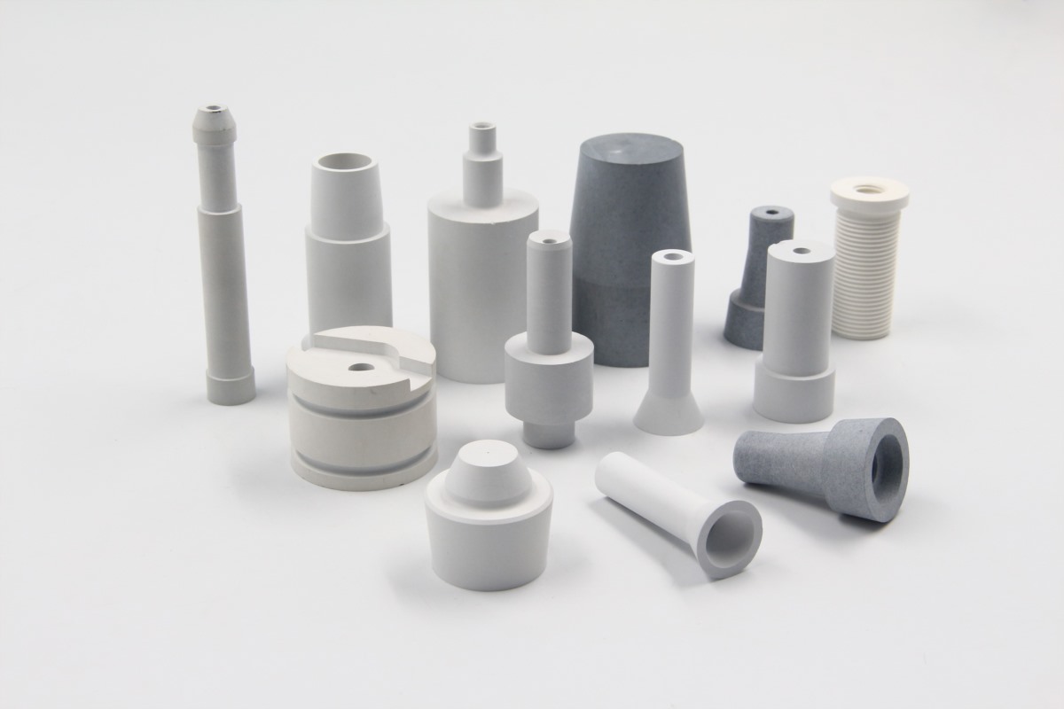
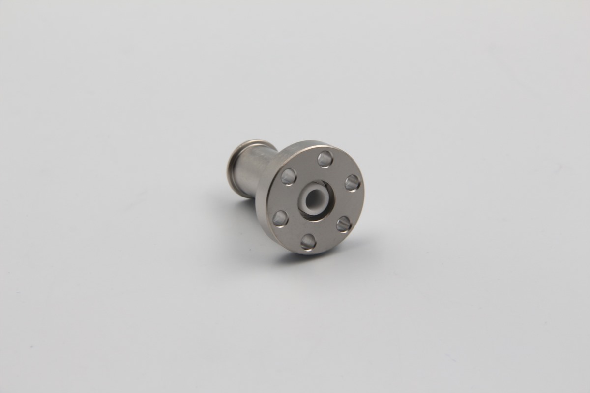
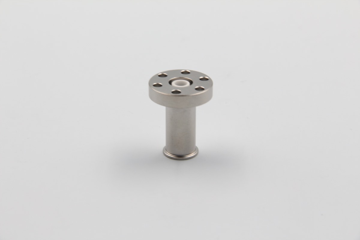
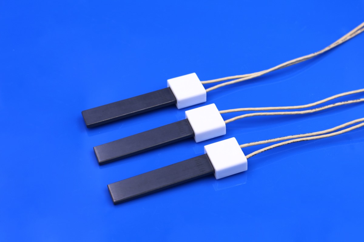
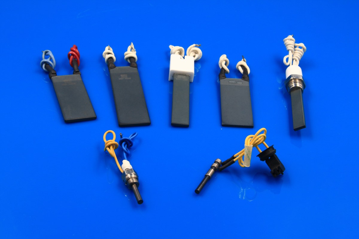
BN Ceramics for PVD ALD and CVD Systems
Talking about the deposition techniques we have to mention Physical Vapor Deposition (PVD), Atomic Layer Deposition ( ALD) and Chemical Vapor Deposition (CVD) , which are fundamental in manufacturing high-precision components for semiconductors, electronics, aerospace industries even more. The versatility and properties of Boron Nitride (BN) ceramics make them become crucial components in PVD, ALD and CVD systems. Here I like to talk about the role of BN ceramics in these systems.
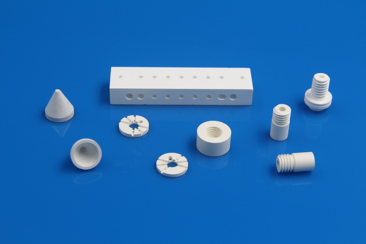
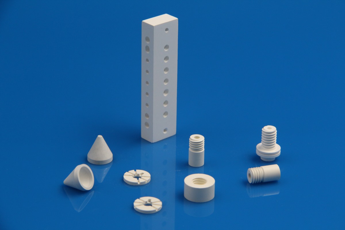
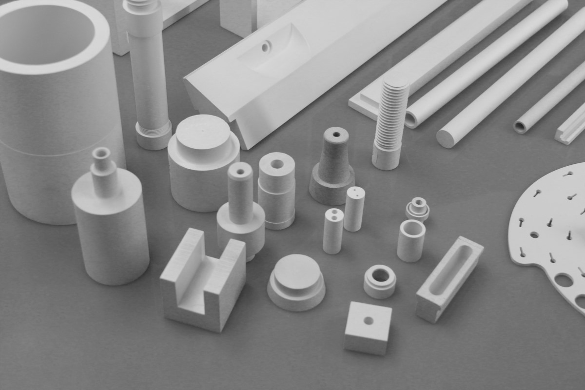
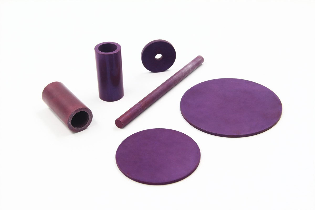
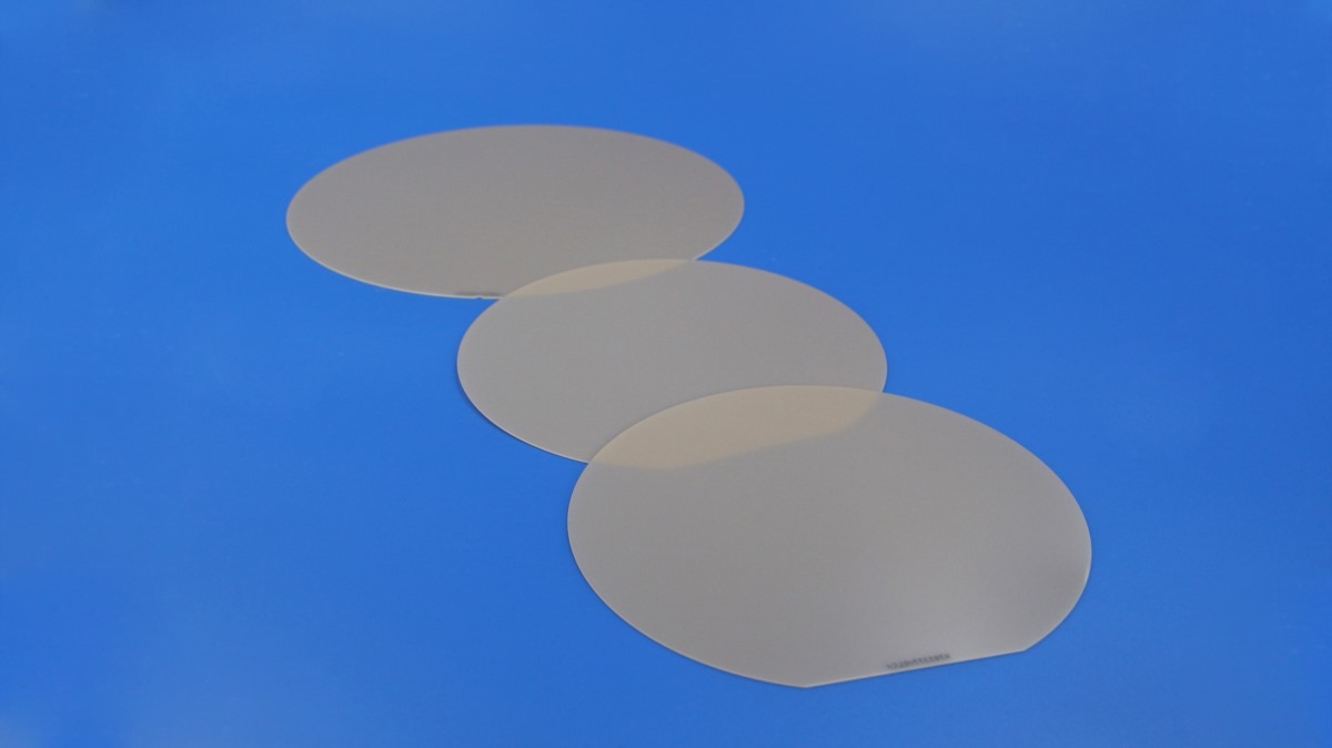
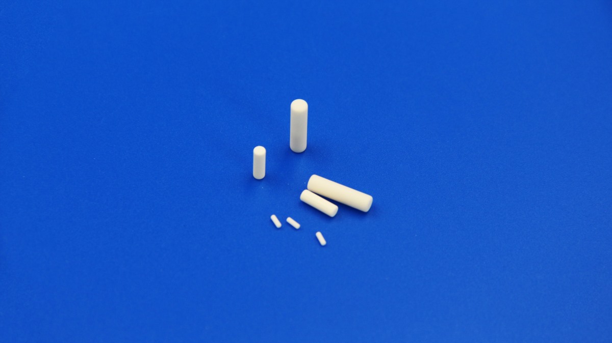
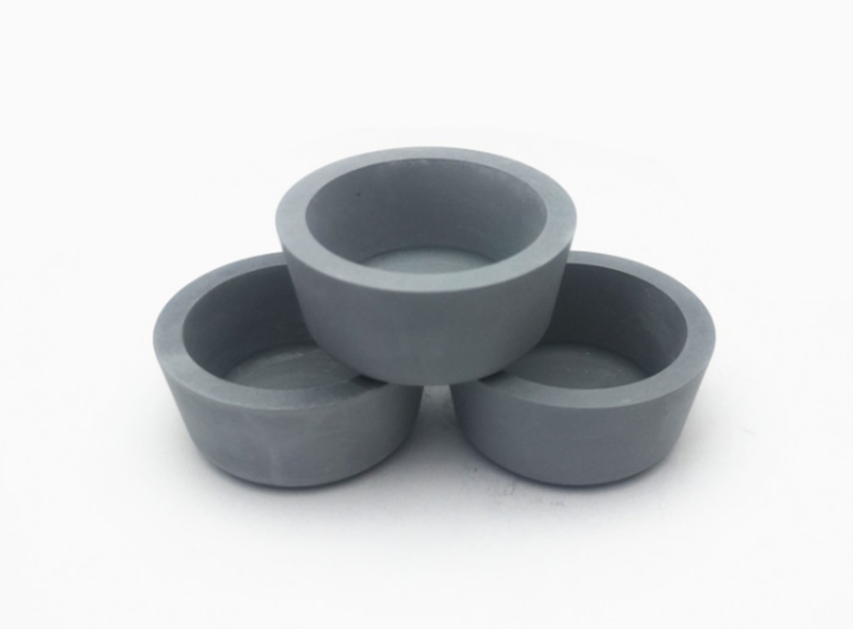
Boron Nitride ceramics are composed of boron and nitrogen atoms arranged in a lattice structure. They can exist in hexagonal (HBN), which is the most commonly used form due to its similarity to graphite, making it an excellent lubricant and insulator. Cubic BN, on the other hand, is known for its hardness, approaching that of diamond.
BN Ceramics in PVD Systems
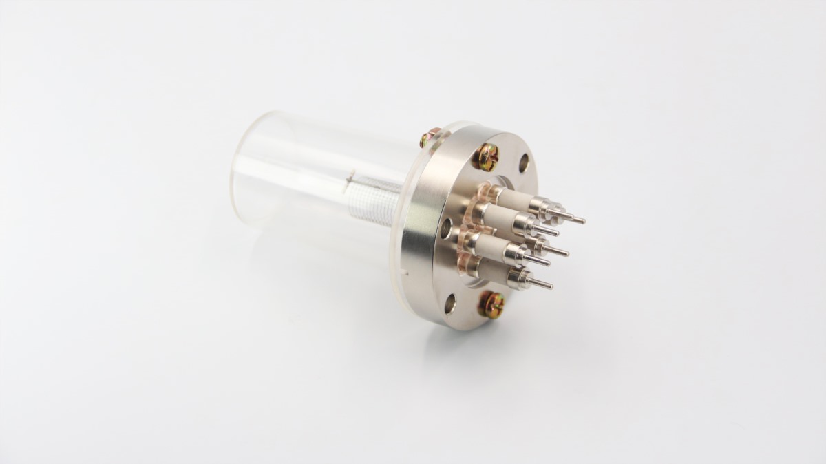
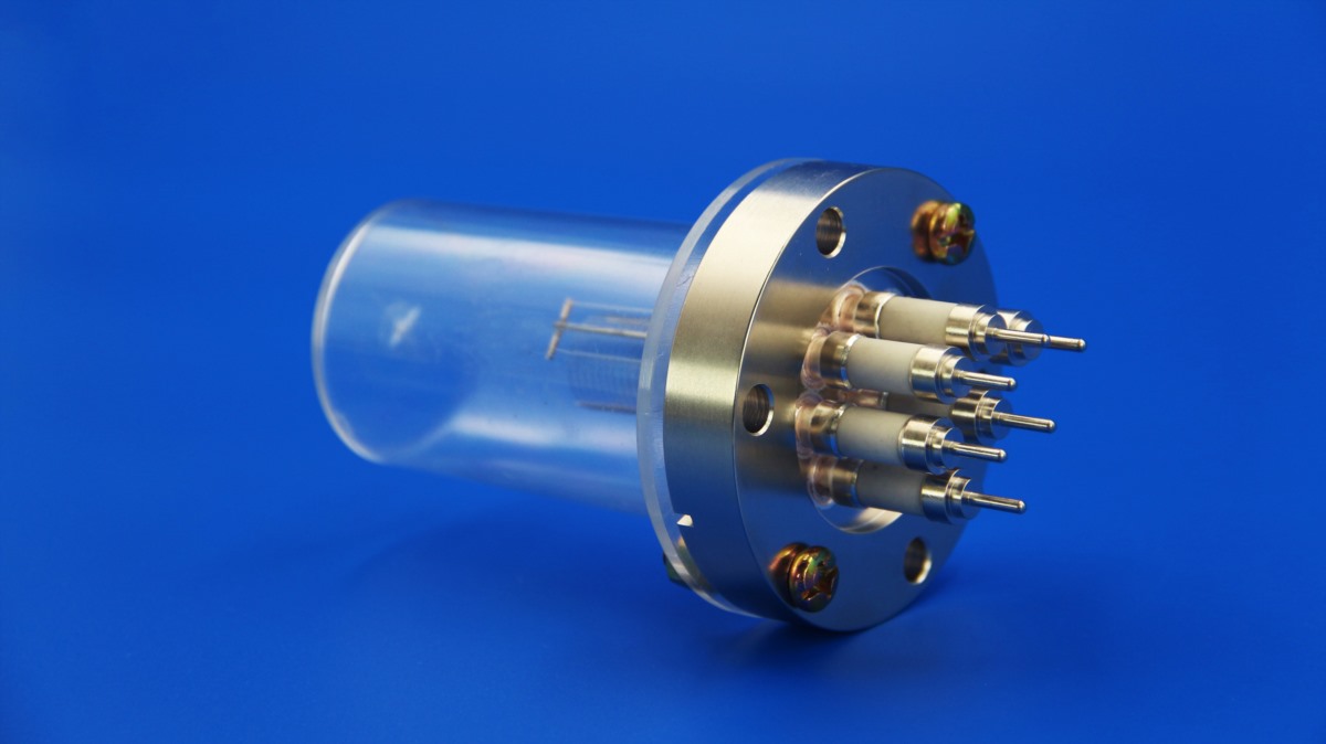
PVD systems are used to deposit thin films through the physical vaporization of material. BN ceramics play a vital role in PVD systems primarily due to their low thermal expansion, chemical resistance, and outstanding electrical insulation.
Low Thermal Expansion: In PVD systems, high temperatures are often required to vaporize materials. BN ceramics shows outstanding thermal stability, allowing them to withstand these high temperatures max about 1800 degree in high vacuum and 2100 degree in in active gas environment without degradation. This property is particularly valuable in maintaining the integrity of the deposition chamber and other components exposed to extreme conditions.
Chemical Resistance: The reactive nature of certain PVD processes can lead to chemical interactions with chamber components. BN ceramics are highly resistant to extreme corrosion and wear, guaranteeing the deposition system remains uncontaminated and operational for longer periods.
Electrical Insulation: BN ceramics is an excellent electrical insulation. It can prevent unneeded electrical discharges during the PVD process. This insulation helps maintain the accuracy and consistency of the deposition process.
BN Ceramics in ALD Systems
ALD is a technique used to deposit thin, conformal films one atomic layer at a time. BN ceramics contribute significantly to the performance and reliability of ALD systems with their low reactivity and stability,help prevent contamination of the film and ensure uniform deposition across complex geometries.
The smooth and clean surface of BN ceramics help minimize particle contamination and defects, which is critical for producing high-quality films in ALD processes. Their non-wetting nature also prevents unwanted interactions with the precursors used in ALD.
BN Ceramics in CVD Systems
CVD involves the chemical reaction of gaseous precursors to form thin films. BN ceramics are integral to CVD systems for their non-reactivity and corrosion resistance that enhance process efficiency and longevity.
CVD processes often involve aggressive gases that can cause corrosion and reaction. BN ceramics exhibit exceptional resistance to these corrosive gases and do not react with them, protecting system components and contamination, extending their lifespan.
Boron Nitride ceramics are very important in enhancing the performance and reliability of PVD, ALD, and CVD systems. Their low thermal expansion, exceptional thermal stability, chemical resistance and outstanding electrical insulation, make them ideal for high-precision deposition processes.


 Enquiry