technical ceramic solutions

News

Category Archives: News

Advantages of Boron Nitride Crucibles in High-Temperature and High-Purity Applications

Hexagonal boron nitride is an excellent self-lubricating ceramic capable of withstanding extremely high temperatures while maintaining its lubricating properties, even in high-vacuum environments. Boron nitride (BN) crucibles are typically manufactured from hot-pressed boron nitride blanks, ensuring high density and structural integrity. Mechanically, hexagonal boron nitride behaves similarly to graphite, but it offers the additional advantage of outstanding electrical insulation.


Compared with graphite crucibles, BN crucibles exhibit significantly lower risk of carbon contamination and demonstrate greater chemical inertness in many high-temperature processes. In comparison with alumina crucibles, BN crucibles show lower wettability to molten metals, making them especially suitable for applications that demand high purity and minimal interaction between the melt and the container. While different crucible materials are optimized for different process conditions, the appropriate selection should always be based on specific operational requirements.


Boron Nitride Ceramic Crucible


BN crucibles are well known for their ability to withstand high temperatures under high-vacuum conditions. In addition, they offer excellent corrosion resistance, thermal stability, and electrical insulation. These properties make boron nitride crucibles an ideal solution for a wide range of advanced industrial and research applications, including:


Crucibles for crystal growth


Laboratory-scale high-temperature synthesis and crystal growth


Semiconductor manufacturing and high-purity metal processing


Vacuum or inert-atmosphere melting of metals and specialty alloys


Sintering and melting of alloys, ceramics, rare earth materials, and other advanced materials


With the continuous advancement of high-temperature processing and high-purity material preparation technologies, the application potential of boron nitride crucibles is steadily expanding. Their role in advanced ceramics, semiconductor fabrication, and emerging functional materials is becoming increasingly significant. Looking ahead, BN crucibles are expected to see broader adoption in more demanding environments involving complex operating conditions and even stricter purity requirements.


Ceramic substrate: The core base material of high-performance ceramic PCB

Currently, electronic products are evolving rapidly towards high power, high integration, and high reliability. The limitations of traditional organic substrates in terms of heat dissipation bottlenecks, high-temperature tolerance and long-term stability are becoming increasingly prominent, and have become a key challenge for industrial upgrading.


In this context, high-performance ceramic substrates, as the core material of ceramic printed circuit boards (ceramic PCB), have become a strategic choice to overcome these bottlenecks and advance power electronics, RF communication, and advanced packaging.


Innovacera, as a manufacturer specializing in advanced ceramic materials, has always been committed to research and development as well as the precise manufacturing of high-performance ceramic substrates. We provide stable, reliable materials and comprehensive support for ceramic PCBs and other high-reliability electronic applications.


Why Ceramic Substrates Are Key to Ceramic PCBs


The overall performance of ceramic PCBs largely depends on the substrate material they use. Compared to traditional organic substrates such as FR-4(Glass Reinforced Epoxy, G10/FR-4), ceramic substrates have significant advantages in several key performance aspects.


1. Excellent heat dissipation capability


Ceramic materials, particularly alumina (Al2O3) and aluminum nitride (AlN), have excellent thermal conductivity, efficiently dissipating heat during operation, reducing junction temperatures, and improving system stability. This characteristic makes it particularly important in power devices and high-power modules.


2. Stable and reliable electrical performance


The ceramic substrate possesses excellent insulation properties and dielectric stability, and can still operate reliably under high voltage and high-frequency conditions. It is an important foundation for the application of ceramic PCBs in the fields of power electronics and radio frequency.


3. Excellent high-temperature resistance and aging resistance properties


Ceramic materials can operate stably at high temperatures for a long time without aging or deforming. They are suitable for use in highly reliable automotive electronics, industrial control, and new energy systems.


4. Excellent dimensional stability


The ceramic substrate offers low thermal expansion and structural stability, meeting the demands of high-precision circuits and high-reliability packaging. It serves as an ideal substrate material for high-end ceramic PCBs.


The crucial role of ceramic substrates in ceramic PCBs


From a structural perspective, ceramic PCBs are essentially circuit systems constructed with ceramic substrates as the core carrier.


The performance of the substrate directly determines the heat dissipation capacity, electrical performance and service life of the entire circuit board.


At present, ceramic substrates have been widely applied in the following ceramic PCBs and related structures:


·DBC (Direct Bonded Copper) substrate
·AMB (Active Metal Brazing) substrate
·thick film / thin film ceramic circuit
·high power LED module
·IGBT and power module packaging


It can be said that high-performance ceramic substrates are the key foundation for achieving highly reliable ceramic PCBs.


Ceramic Substrates


Innovacera Ceramic Substrate Solution


With proven materials and stable manufacturing processes, Innovacera offers a wide range of high-performance ceramic substrates for diverse applications.


■ Alumina (Al2O3) ceramic substrate


Stable performance, high cost-effectiveness, widely used in electronic packaging, LED modules, and general power devices.


■ Aluminum nitride (AlN) ceramic substrate


It has excellent heat-conducting properties and is suitable for high-power density applications, such as power modules, communication equipment and new energy systems.


Silicon nitride (Si3N4) ceramic substrate


It combines high strength and high reliability, and is suitable for application environments with high requirements for mechanical properties and thermal shock.


■ ZTA (zirconia-reinforced alumina) ceramic substrate


While maintaining the excellent insulation properties of alumina, the introduction of zirconia phase significantly enhances fracture toughness and impact resistance, suitable for electronic and industrial applications that demand high mechanical toughness, wear resistance, and structural reliability.


Meanwhile, Innovacera can provide customized ceramic substrates of various sizes, thicknesses and surface treatment methods according to customer requirements, providing a reliable foundation for the subsequent ceramic PCB manufacturing and packaging processes.


A reliable choice for high-end electronic applications


With the rapid development of new energy, 5G communication, power semiconductors and high-end equipment manufacturing, the market demand for high-performance ceramic substrates continues to increase.


As the core material of ceramic PCBs, ceramic substrates play an increasingly important role.


Backed by proven material systems, mature manufacturing processes, and extensive application experience, Innovacera delivers high-quality ceramic substrate solutions to support the reliability and performance of next-generation electronics.


Beyond Light Blocking: Anti-Static Advantages of Black Alumina Ceramics in Optoelectronic Packaging

As optical communication, LiDAR, and high-precision optoelectronic detection systems evolve toward higher power and greater integration density, they place higher demands on the performance of optoelectronic packaging materials. The increase in device power brings challenges in heat dissipation and high-temperature stability, while the improvement in integration density raises the risks of internal stray light interference and electrostatic discharge (ESD), directly affecting system reliability and signal-to-noise ratio. Traditional white alumina has limitations in optical control, and conventional ESD protection solutions often fail to be perfectly compatible with high gas-tightness and high thermal conductivity packaging systems.


Based on the high mechanical strength, thermal conductivity, and excellent insulation properties of black alumina ceramics, the material achieves a multi-functional integration of optical control, thermal management, and on-chip electrostatic discharge (ESD) protection.


Black Alumina Ceramics


1. Anti-static capability: Material-level ESD protection


Black alumina ceramics achieve this controlled resistivity by precisely doping transition metal ions (such as manganese, titanium, and cobalt) at the boundaries of the alumina grains, thereby forming a microscopic conductive network within the material. As a result, the volume resistivity of the material can be controlled within the range of 10⁶ – 10¹¹ Ω·cm.


This design enables the electrostatic charges to be released at a controlled and gradual rate, preventing damage to the laser or photodetector chips due to instantaneous discharge, while also not affecting the signal integrity. Compared with applying anti-static coatings or conductive fillers on the surface, the intrinsic conductive properties of black alumina ceramics


2. Optical Control and Thermal Management: The Comprehensive Advantages of Black Ceramics


Black alumina ceramics achieve high absorption rates for visible light and near-infrared light through ion doping, which can increase the absorption rate of internal stray light in the package to over 95%. This effectively reduces optical crosstalk and noise, providing a stable optical environment for high-speed optical communication modules and precise photodetectors.


Meanwhile, it inherits the high mechanical strength and high thermal conductivity (approximately 24–28 W/(m·K)) of white alumina ceramics. It efficiently dissipates heat from the device, maintaining dimensional stability and performance under high-power, high-temperature conditions, ensuring long-term reliable operation.


3. Multi-functional Integrated Application Cases


(1)High-Power Laser Module Packaging


• Black alumina ceramic can be used as a tube shell or heat sink, efficiently conducting the heat from the chip.


• The black ceramic body absorbs reflected light, reducing optical interference.


• Its ESD control properties protect the chips during mounting and wire bonding.


(2)Avalanche Photodiode (APD) Packaging


APD is highly sensitive to static electricity. Black alumina ceramic, when used as a tube base or window plate, can provide physical support, optical isolation, thermal management and static shielding, significantly enhancing the component’s surge resistance and operational lifetime.


(3)Microwave Optoelectronic Integrated Modules


• The module integrates a laser, a driving circuit and a radio frequency transmission line. The electromagnetic environment is complex.


• The black alumina ceramic substrate combines microwave transmission performance, electrostatic discharge prevention function and optical signal isolation, achieving the integration of a multi-functional substrate.


Black Alumina Ceramics parts


The multi-functional integration characteristics of black alumina ceramics signify the evolution of photonic packaging materials from passive protection to active functional design. It has been optimized through materials science, integrating optical control, thermal management and anti-static functions, providing a system-level reliability solution for high-power and high-integration optoelectronic devices.


For photonic systems that aim for high performance and ultra-high reliability, choosing black alumina ceramics is not just selecting a packaging material—it represents a system-level high-reliability strategy. Innovacera provides customized solutions for ceramic packages using black alumina ceramics—contact sales@innovacera.com
to learn more.


Boron Nitride Evaporation Boats: Ideal Ceramic Components for High-Temperature Vacuum Applications

The boron nitride evaporation boat (BN evaporation boat) is a high-temperature device made of high-purity hexagonal boron nitride ceramics. It is usually in a boat shape or custom-made, and can hold various evaporation materials. During use, it not only serves as a container for holding molten materials but also maintains the cleanliness and stability of the working environment. Unlike ordinary ceramic components, the BN evaporation boat possesses both structural strength and chemical inertness, and can be used stably for a long time under extreme conditions.


BN evaporation boat


The comprehensive advantages of materials and techniques


(1) Core material: High-purity hexagonal boron nitride


Its purity is ensured not to have any impurities precipitate at high temperatures, fundamentally eliminating the pollution caused by the vessel, maintaining extremely high purity of the evaporated material, and ultimately achieving high-purity and high-performance thin film deposition. Therefore, it fully meets the strict requirements for film layer quality in high-precision industries such as semiconductors and optical coating.


Unreplaceable material performance advantages


h-BN is hailed as “white graphite”, possessing a variety of outstanding properties:


•High temperature resistance: Can be used stably in the air up to approximately 900℃, and can withstand temperatures above 2000℃ in vacuum or inert atmospheres.


•Chemical inertness: Does not react with most molten metals, semiconductor materials, glass, or chemical gases.


•Non-adhesive and non-wetting properties: The molten material forms beads on the BN surface, which are easily spilled or completely evaporated, leaving very little residue. The material utilization rate is high, and it is convenient for cleaning and maintenance.


•Thermal shock stability and insulation: Can withstand frequent thermal cycling while maintaining structural integrity; also an excellent high-temperature insulator, suitable for various heating methods.


Compared with graphite or metal evaporation vessels, BN evaporation vessels demonstrate significant overall advantages due to their unique chemical inertness and thermal stability. It not only withstands high temperatures and is resistant to corrosion, eliminating the risks of oxidation and contamination, but also significantly reduces material residue due to its non-wetting and non-adhesive surface. This improves the evaporation efficiency, extends the service life, and ensures the high stability and consistency of the process.


(2) Key Process: Vacuum Hot Press Sintering


This process can uniformly densify BN powder under high temperature and high pressure, thereby forming a microscopic structure with extremely stable physical properties. Its direct advantage lies in:


• Significantly enhance the bending strength and thermal shock resistance


• Extend service life and reduce replacement frequency


Boron Nitride Ceramic


(3) Multi-form application, providing comprehensive solutions


Based on the excellent and universal performance of h-BN, it is not only fabricated into evaporation vessels, but also processed into various forms of high-temperature components, serving a wider range of fields:


• Ceramic rod: Used for stirring high-temperature molten materials.


• Ceramic plates, blocks, and crucibles: Used as high-temperature support platforms, sintering pads, or melting containers.


• Various customized components: such as high-temperature insulating isolation parts, pouring nozzles, protective sleeves, etc.


These products collectively offer a complete and reliable material solution for experiments and industrial environments that require high temperatures, chemical corrosion resistance, high purity, and electrical insulation.


The application scenarios of the BN evaporation boat


The core application of the BN evaporation boat is focused on areas that have extremely strict requirements for material purity, process stability, and equipment durability. These mainly include:


1. Semiconductor and Microelectronics Manufacturing


Key process: Vacuum evaporation deposition for components such as integrated circuits and sensors.


Specific application: evaporating high-purity metal interconnects (such as aluminum and gold), and functional film layers is a critical step in chip manufacturing.


2. Optical and Display Industry


Key process: Precise optical coating and conductive film preparation.


Specific applications: depositing anti-reflective, reflective, and other multi-layer optical films on lenses, lasers, and filters; preparing aluminum electrodes and ITO conductive films for display panels to ensure purity and uniformity of the film layers.


3. High-purity material research and special processing


Key process: Material synthesis and processing under high-temperature and high-purity conditions.


Specific applications:


Melting, evaporation and refining of metals and alloys (such as aluminum, gold, silver, chromium).


Purification and crystallization of high-purity substances under an inert atmosphere.
Used as an inert crucible or support piece for the high-temperature preparation of special glasses and crystals.


4. Surface Engineering and Functional Coatings


Key process: Decorative and functional surface coatings.


Specific application: On the surfaces of tools, consumer goods, etc., deposit protective, decorative, or functional special film layers.


With its numerous outstanding properties, the BN (boron nitride) evaporation boat plays an irreplaceable role in modern vacuum evaporation, thin film deposition, and semiconductor manufacturing processes. For process scenarios that require high reliability, high purity, and long lifespan, the BN evaporation boat is a mature and reliable engineering ceramic solution. Innovacera offers customized services for various specifications of BN evaporation vessels, which can meet the requirements of various high-temperature vacuum processes and provide customers with high-quality technical support and after-sales guarantees.


Vacuum Electrical Power Feedthroughs for High-Performance Vacuum Applications

In a vacuum environment, the pivotal conduit for secure energy transmission.


Vacuum electrical power feedthrough is a key through component specially designed for vacuum systems. Its core function is to safely and reliably transfer electrical energy from the atmospheric environment to the vacuum interior while absolutely maintaining the vacuum seal of the cavity. It is the indispensable “energy link” that connects the external power source with the internal load of the cavity.


This component has solved the core problem of stable power supply under high vacuum conditions, and is the foundation for the reliable operation of various heating, high-voltage, and particle beam processes.


Vacuum Electrical Power Feedthroughs


Design core: Sealing, insulation and current carrying capacity


The design of vacuum electrical power feedthrough is centered around three core aspects: sealing, insulation, and current-carrying capacity.


(1) Based on the mature ceramic-metal brazing technology, an atomic-level airtight connection is achieved, meeting the requirements of high vacuum and ultra-high vacuum applications. It also exhibits long-term stability under high-temperature baking and harsh working conditions.


(2) Robust mechanical and electrical structure: 304/316L stainless steel flanges, compatible with CF, KF, and ISO standard interfaces; conductors made of oxygen-free copper, copper-nickel alloy, or Kovar alloy, optionally gold or nickel plated to reduce contact resistance. High-purity aluminum oxide ceramic provides reliable insulation and thermal stability.


(3) Flexible electrical performance configuration: It supports configurations ranging from single conductors and dual conductors to multi-conductor arrays, meeting the requirements for single-channel or multi-channel independent power transmission. Depending on the application, it can be classified as high current type, high voltage type or composite power type. It can not only transmit hundreds of amperes of high current, but also withstand tens of thousands of volts of high voltage, providing reliable power support for complex vacuum processes.


Vacuum Electrical Power Feedthroughs


Core product advantages:


Absolutely reliable airtight guarantee: Permanent metalization sealing effectively eliminates the risk of air leakage, ensuring the lifespan and process purity of the vacuum system.


Extensive parameter coverage: Voltage, current, the number of conductors, flange type, and installation dimensions can all be highly customized to precisely match the customer’s system blueprint.


Tolerance to extreme environments: The working temperature range is wide, it is resistant to particle irradiation, and can adapt to plasma and corrosive atmospheres.


Standardized and convenient integration: Compliant with international vacuum flange standards, it can be installed immediately upon arrival, significantly shortening the equipment design and installation cycle.


Durable and stable performance: Composed entirely of inorganic materials, it has no aging phenomenon and an extremely low gas emission rate, ensuring that the equipment can operate without maintenance throughout its lifecycle.


Typical application scenarios:


Vacuum evaporation coating (PVD/CVD) equipment: Safety connection of the heating power supply or anode-cathode power supply.


Vacuum furnace and heat treatment system: Supply power to the heating elements or control module inside the cavity.


Electron beam and ion beam equipment: High-voltage power is supplied to the interior of the chamber for particle acceleration or deposition processes.


Vacuum testing and analysis equipment: Such as SEM (Scanning Electron Microscope) and mass spectrometers, which achieve multi-channel electrical connections.


Vacuum electrical power feedthrough is a comprehensive product that integrates ultra-high vacuum technology, materials science, precise brazing techniques and high-voltage insulation design. Its performance directly determines the processing capability, reliability and safety of the vacuum equipment. A reliable feedthrough is the stable “energy core” of a vacuum system.


Innovacera is committed to providing comprehensive support, from standard feedthrough products to fully customized solutions, safeguarding your innovative research and development and large-scale production.


Aluminum Nitride (AlN) Ceramic Substrates for Efficient IGBT Module Cooling

Behind the swift movement of electric vehicles, the operation of photovoltaic power stations, and the precise control of industrial production lines, there is a common core power component – the IGBT (Insulated Gate Bipolar Transistor) module. It converts direct current into alternating current, precisely regulates the motor speed and torque, efficiently controls power switches, and completes the conversion and regulation of electrical energy. It is the “heart” of power electronic devices.


As the industry continuously enhances the performance and efficiency of systems, IGBT modules are evolving towards higher power density, smaller size, and greater reliability to meet the demands of lightweighting in electric vehicles, high power output, efficient operation of new energy inverters, as well as long lifespan and high reliability of industrial frequency conversion equipment. In such applications with high power and high heat load, safely and efficiently discharging the heat generated by the chip has become a major challenge in module design.


This answer is largely hidden within a seemingly insignificant component of the module – the base plate. It is not an ordinary metal plate, but a precise component made of a copper-ceramic-copper composite structure. The substrate of IGBT modules has traditionally been made of ceramic materials. For low-power modules, aluminum oxide, which is cost-effective and has mature manufacturing processes, is commonly used. However, in high-power and high-reliability applications, aluminum nitride has emerged as the key material for modern IGBT substrates due to its high thermal conductivity and excellent insulation properties.


Why aluminum nitride?


Aluminum Nitride (AlN) Ceramic Substrates


Aluminum nitride is an advanced functional ceramic. It is used in high-performance IGBT modules due to its outstanding physical properties:


(1) Excellent thermal conductivity: The thermal conductivity is as high as 170–230 W/mK, which is 6–8 times that of traditional alumina, enabling the rapid transfer of heat generated by the chip to the base plate, thus preventing overheating and failure.


(2) Reliable insulation: While achieving efficient heat conduction, AlN maintains a high volume resistivity and dielectric strength, enabling the construction of a stable electrical isolation barrier at the typical operating voltage of IGBT modules, ensuring operational safety.


(3) Matching thermal expansion: Its thermal expansion coefficient (~4.5×10⁻⁶/K) is close to that of silicon chips. During thermal cycling, it effectively reduces thermal stress and prevents the cracking of the soldering layer, thereby enhancing long-term reliability.
However, merely having high-performance ceramics is not sufficient to construct a complete module. It needs to be combined with metals in order to conduct current and dissipate heat.


DBC Technology: From Ceramics to Multi-functional Substrates


In order to fully utilize the material advantages of AlN, modern IGBT modules typically employ the Direct Bonded Copper (DBC) technology. This process achieves the bonding of high-purity copper foil firmly to both sides of the AlN ceramic sheet through a high-temperature eutectic reaction, forming a sandwich structure of copper-ceramic-copper. Each layer has a clear and coordinated function:


-Upper copper layer: As the circuit layer, it is used for soldering IGBT chips and conducting the main current.


-The middle AlN ceramic layer: It is the functional core, achieving both efficient insulation and rapid heat conduction.


-Lower copper layer: As a heat transfer layer, it conveys heat to the metal base plate and the external cooling system.


Through this structure, the AlN-DBC substrate is no longer an isolated ceramic, but becomes a multifunctional integrated carrier that integrates conductivity, insulation, heat conduction and mechanical support, laying a solid physical foundation for the high power density and high reliability operation of IGBT modules.


The core mission of AlN-DBC


In the IGBT module, AlN-DBC determines the performance limit of the module:


(1) Thermal Management
The high thermal conductivity enables the heat generated by the chip to be quickly dissipated, ensuring the stable operation of the module under high current and high power density conditions, and achieving miniaturization and high efficiency.


(2) Electrical insulation
Provide reliable insulation isolation between high-voltage chips and the grounding heat sink to ensure the safe operation of the high-voltage system (such as the automotive 800V platform).


(3) Mechanical Stability
The thermal expansion matching reduces thermal cycling stress, ensuring the interface reliability of the module during frequent start-stop, acceleration, and high-power cycles, significantly extending its service life.


For this reason, AlN-DBC has become the preferred solution for advanced applications such as electric vehicle main drive inverters, on-board chargers (OBC), high-power photovoltaic/storage converters, ultra-fast charging stations, and high-end industrial servo drives. It provides a solid material foundation for performance breakthroughs in these fields.


With the development of power electronics technology, IGBT modules are evolving towards higher power, smaller size and greater reliability. The AlN-DBC substrate provides crucial support for this trend and lays the foundation for future high-temperature applications of wide bandgap semiconductor devices. Innovacera can offer customized solutions for Aluminum nitride (AlN) Substrates, helping customers create high-performance and reliable next-generation power modules. Please feel free to contact us.


HTCC Ceramic Packaging Technology: The Key to High Power and High Frequency Applications

In the modern electronics industry, the three types of ceramic packaging and component technologies, namely HTCC, LTCC and MLCC, jointly form the foundation of high-performance electronic systems.


Although they all belong to the multi-layer ceramic technology system, their application directions and performance emphases are different:


HTCC is used for high-reliability and high-power packaging, LTCC excels in integrating high-frequency and multi-functional circuits, and MLCC is the core type of surface-mount passive components.


These three factors jointly support the high performance and miniaturization development of modern electronic devices.


This article mainly introduces the HTCC packaging technology:


HTCC Ceramic Packaging


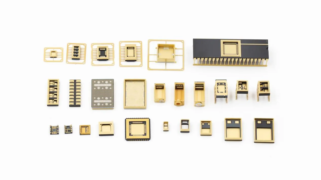
HTCC packaging combines alumina or aluminum nitride porcelain wafers with tungsten/molybdenum metal circuits through a set of precision ceramic-metal co-firing process, and finally forms a high-density, highly reliable three-dimensional ceramic circuit structure through key steps such as molding, printing, co-firing and packaging.


The key steps include:


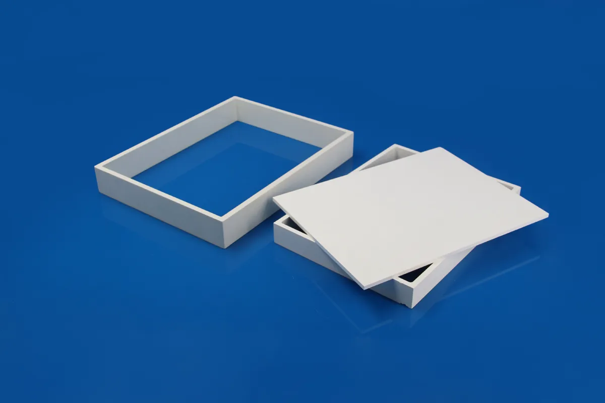
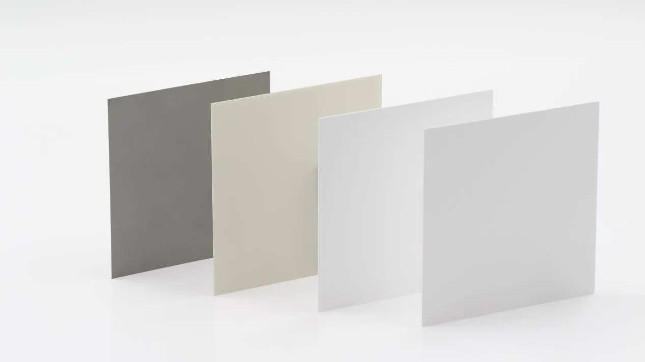
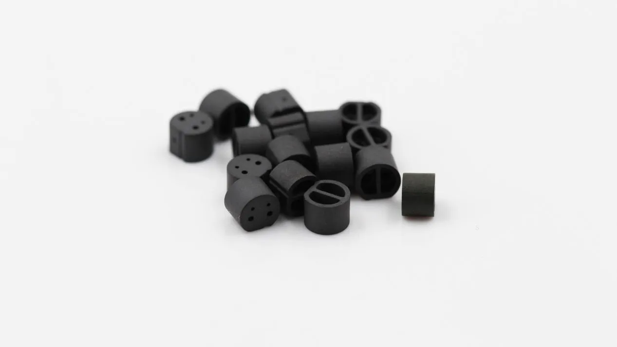
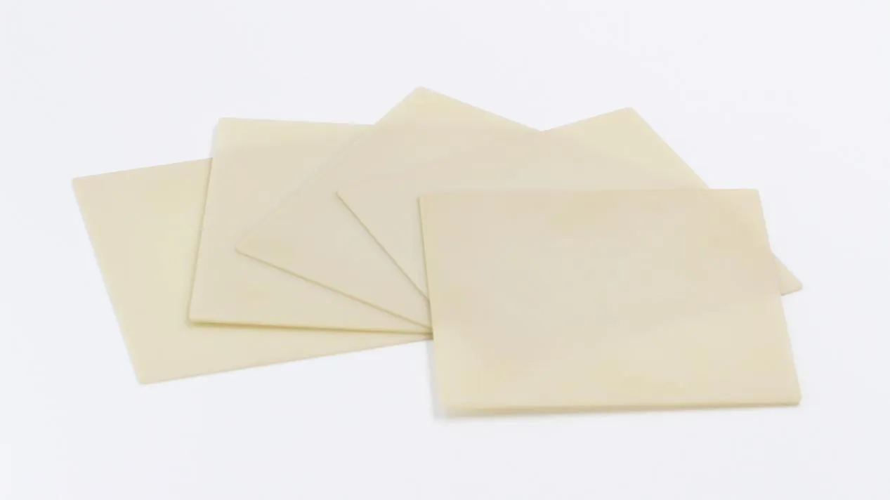
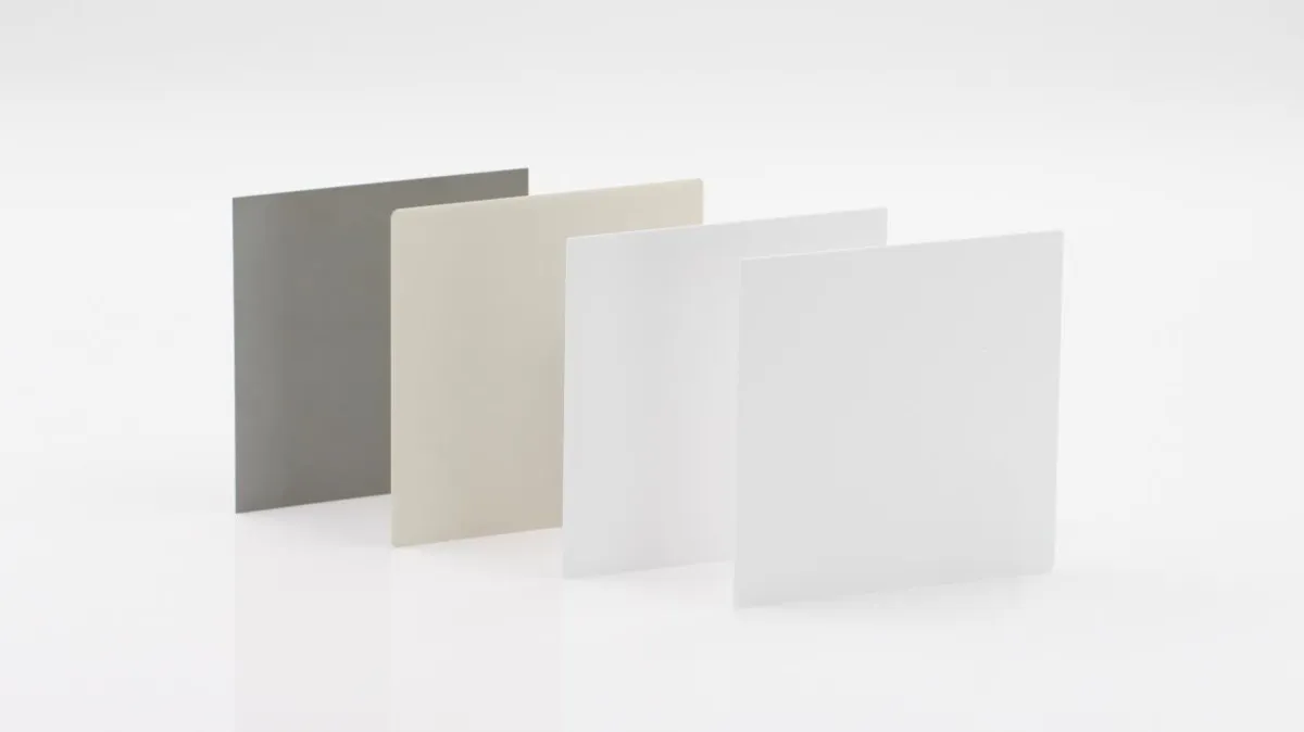
(1) Ceramic substrate preparation (tape casting):


Mix the ceramic powder (such as alumina) with organic binders, plasticizers and solvents to form a uniform slurry. Then, use a casting machine to shape it into a certain thickness of raw porcelain sheet.


This step requires strict control of drying conditions and slurry viscosity to ensure uniform thickness and flat surface of the raw film, providing a stable foundation for subsequent printing and lamination.


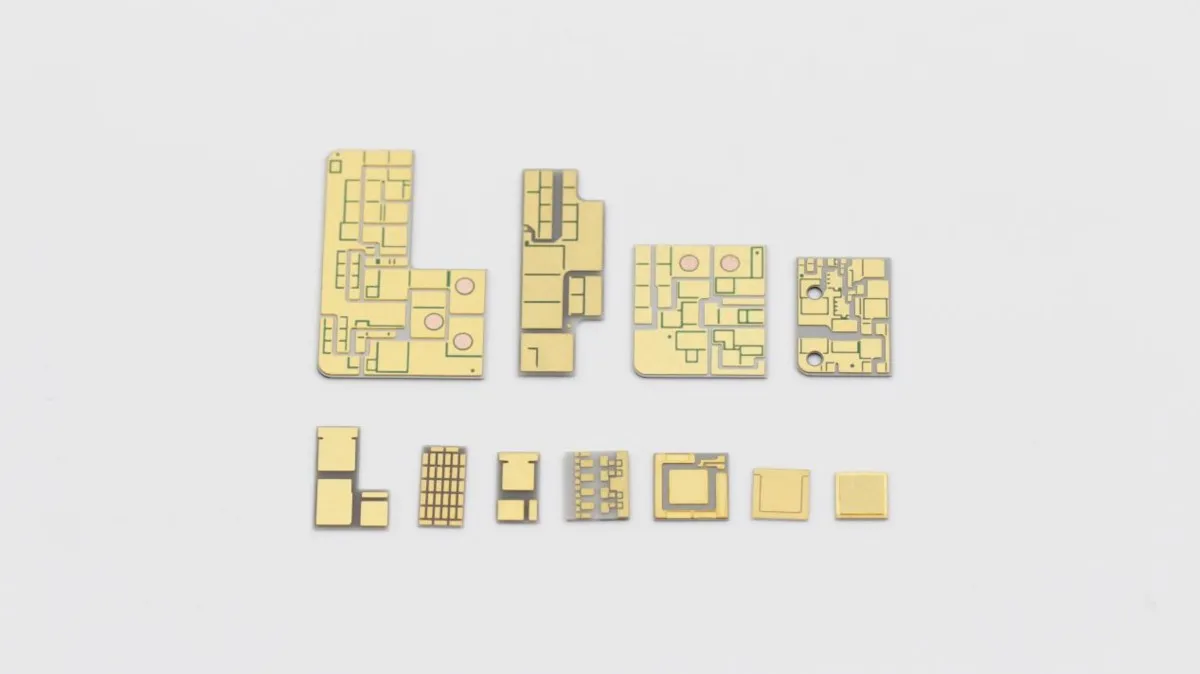
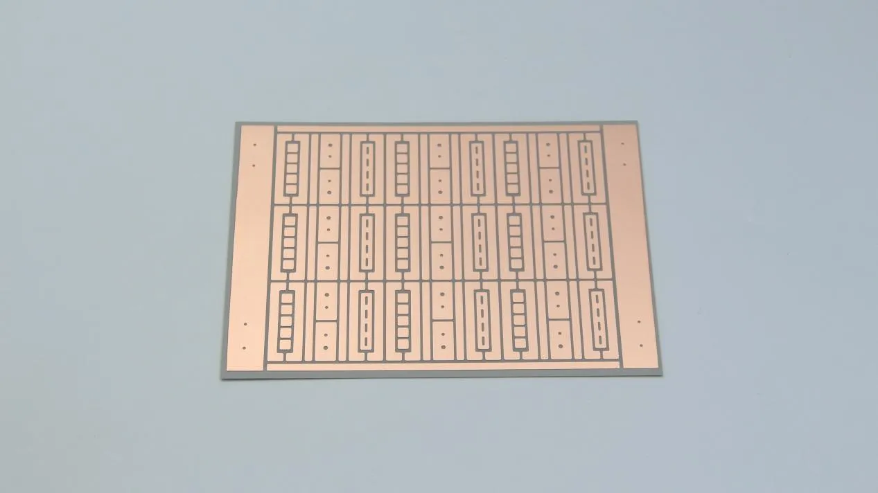
(2) Circuit Printing:


Conductive lines and through-holes are formed on the surface of the raw porcelain pieces through the screen printing process. Using tungsten, molybdenum or their alloys as the metal conductor enables it to withstand the subsequent high-temperature co-firing process.


After printing, it is usually dried and degreased at low temperature to ensure that the metal circuit is firmly adhered to, the pattern is clear, and there are no bubbles and impurities.


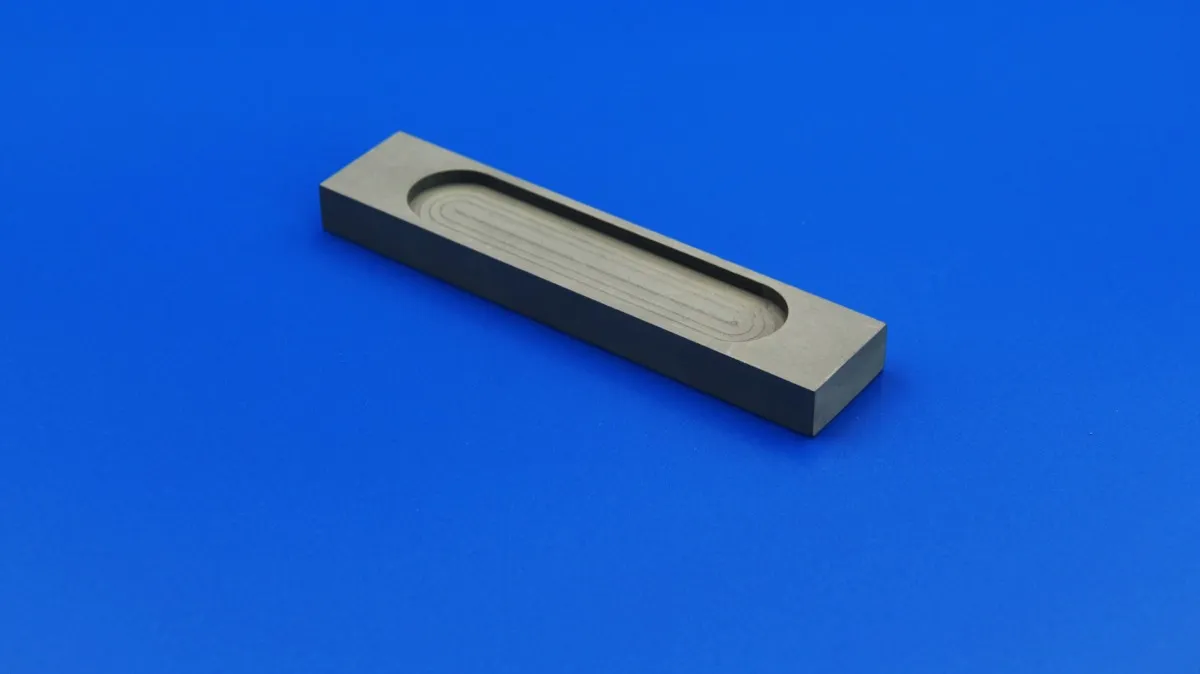
(3) Layering and Lamination:


The printed multi-layer preforms are precisely aligned and overlapped, and the interlayer bonding is achieved through heat pressing or isostatic pressing techniques to form a three-dimensional interconnection structure.


The accuracy of this step directly affects the size tolerance of the finished product and the reliability of conduction.


(4) High-temperature co-firing:


In a reducing atmosphere, the ceramics and metal conductors are sintered together at a temperature of around 1600℃ to achieve synchronous densification, thereby forming a robust multi-layer substrate.


The finished product usually undergoes a volume contraction of approximately 15—20%, so compensation for this shrinkage needs to be taken into account during the design stage.


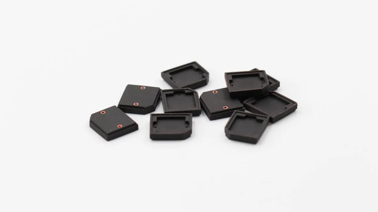
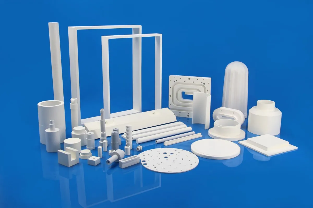
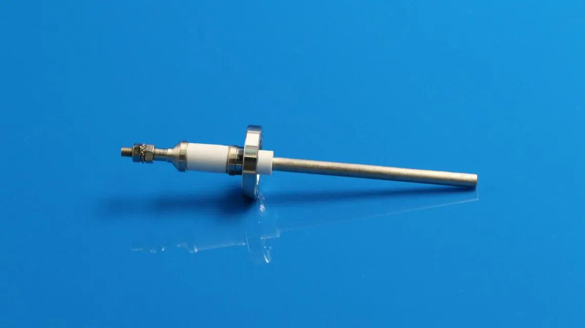
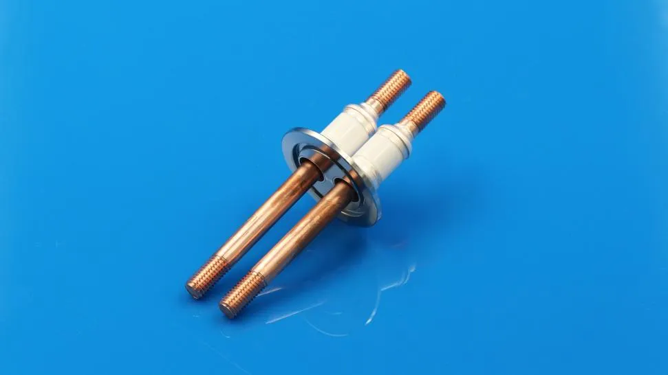
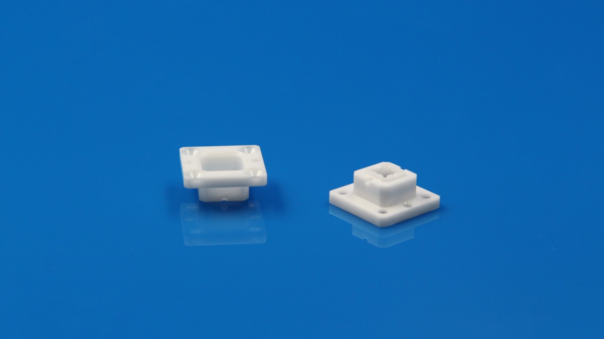
(5) Post-processing techniques:


Carry out processing such as metallization, electroplating, cutting, welding, pin installation or gas sealing on the sintered substrate.


Some of the high-end HTCC products will also undergo solder pre-coating, electrode strengthening or laser marking to meet the demanding requirements of medical or high-temperature electronic applications.


Technical Advantages


· Excellent high-temperature stability


The HTCC package can operate stably for a long time in an environment of 300–350°C.


With special design, it can even withstand short-term extreme high temperatures above 400°C.


Its ceramic framework maintains structural integrity and airtightness at high temperatures, which is crucial for achieving high-temperature electronic packaging.


· Outstanding electrical insulation property


The ceramic matrix itself is an excellent insulating material, featuring low dielectric constant and low dielectric loss, which helps ensure the integrity of high-frequency signal transmission and reduces interference.


· High mechanical strength and environmental durability


The structure is sturdy and can withstand thermal shock, mechanical vibration and corrosive environments.


Its reliability is much higher than that of ordinary plastic packaging and it is suitable for use in harsh conditions such as industrial and aerospace applications.


· Support high-density three-dimensional integration


By stacking multiple layers of porcelain tiles and achieving vertical interconnection, a complex three-dimensional wiring structure can be realized, supporting high pin count, high frequency and miniaturized packaging designs.


· Excellent thermal management performance


Ceramic materials (especially aluminum nitride, AlN) have a high thermal conductivity, which can effectively transfer the heat generated by the chip, thereby increasing the power density and service life of the device.


Application Fields


· Automotive electronics: Applied in engine control modules (ECU), pressure sensors and on-board power modules to cope with the high temperatures and vibrations within the engine compartment.


· Industry and Energy: Provides services for core power conversion equipment such as frequency converters and inverter power supplies, ensuring their long-term operation under high temperatures and high power densities.


· High-frequency communication: As the RF circuit and filter carrier in 5G base stations and radar systems, it ensures the low-loss transmission of high-frequency signals.


· Sensor technology: Provides sturdy and airtight packaging shells for various MEMS, gas, infrared and pressure sensors, suitable for harsh conditions.


· High-end equipment: It is the key packaging solution for highly reliable control systems in aerospace, and implantable medical devices.


Thus, whether it is to cope with harsh environmental challenges or to achieve the ultimate performance, HTCC ceramic packages offers a proven and reliable path.
When your project is subjected to demanding conditions such as high temperature, high frequency, high power or long-term reliability, HTCC might just be the key solution.
INNOVACERA is dedicated to providing customers with professional HTCC ceramic packaging solutions. Please feel free to contact us.


Why choose zirconia ceramics as a thermal insulation plate?

Zirconia (ZrO₂) ceramics are widely used as thermal insulation plates thanks to their excellent thermal insulation performance, high mechanical strength, and outstanding stability at elevated temperatures. The excellent insulation performance of zirconia ceramics comes from their intrinsically low thermal conductivity, which effectively reduces heat transfer. As a result, zirconia insulation plates are commonly employed in various industrial systems that require reliable thermal barriers.
Below are the key features and advantages:


High-Speed Capability

Zirconia ceramics offer strong cold resistance, low elastic modulus, high compressive strength, low thermal conductivity, light weight, and a low coefficient of friction. These properties allow them to be used in high-speed spindles operating from 12,000 to 75,000 rpm as well as other high-precision equipment.


Zirconia sheets


High Temperature Resistance

Zirconia insulation plates maintain stable performance with minimal thermal expansion across 500–600 °C, making them suitable for applications exposed to significant temperature fluctuations.


Zirconia ceramics parts


Corrosion Resistance

Due to their inherent chemical stability, zirconia ceramics resist corrosion from strong acids, strong alkalis, inorganic salts, organic salts, and seawater. This makes them ideal for electroplating equipment, electronic devices, chemical machinery, shipbuilding, and medical equipment.


Antimagnetic Properties

Zirconia insulation plates are non-magnetic and do not attract dust, reducing premature wear, shaft spalling, and operational noise. They are suitable for demagnetization equipment, precision instruments, and other applications requiring non-magnetic components.


Electrical Insulation

With high electrical resistivity, zirconia ceramics help prevent arc damage to shafts and can be used effectively in electrical equipment requiring stable insulation performance.


Vacuum Compatibility

The self-lubricating, oil-free nature of zirconia ceramics overcomes the lubrication challenges faced by ordinary ceramic plates in vacuum environments, making them suitable for vacuum systems and related equipment.


In addition, zirconia ceramic insulation plates offer excellent impact and wear resistance, contributing to their long service life and overall durability. INNOVACERA manufactures a wide range of zirconia components, allowing users to select products based on specific performance and application requirements. For customized insulation solutions, feel free to contact us.


Pain Points in Thick- and Thin-Film Circuit Fabrication and Ceramic Substrate Advantages

In the pursuit of high performance and high reliability in electronic manufacturing, traditional substrate materials have become increasingly unable to meet the ever more demanding requirements. Limited thermal conductivity, poor high-temperature stability and insufficient surface accuracy are becoming the bottlenecks for the development of thick-film and thin-film circuits. Therefore, the industry urgently needs a new type of carrier that combines excellent insulation, efficient heat dissipation, outstanding dimensional stability and ideal surface flatness to support the printing and sintering processes of precision circuits.


Core performance requirements of thick film/film circuits for the substrate:


In the field of high-performance electronics, thick-film and thin-film circuits are two crucial microfabrication technologies. Although their processing paths are different, they both impose many similar and stringent requirements on the substrate materials that carry their circuits.


Metallized ceramic circuit board


The thick-film circuit is formed by applying conductive, resistive or insulating pastes through screen printing on the surface of the substrate, and then undergoing high-temperature sintering for solidification to create the circuit pattern. The typical sintering temperature is approximately 850℃ – 900℃, and the specific temperature depends on the type of slurry and the substrate. The core of its process requires that the substrate must be able to withstand high-temperature thermal shock, maintain extremely high dimensional stability (without warping or shrinking) and chemical inertness during the sintering process, prevent reactions with the paste, and at the same time, the surface must meet the required flatness and adhesion for printing.


The thin-film circuit adopts processes such as vacuum coating, lithography and etching to fabricate fine lines at the micrometer or even nanometer scale on the substrate. This requires that the surface of the substrate have an extremely low roughness (almost atomic-level smoothness) to ensure the precise formation of the circuits, and it must have excellent uniformity of microstructure and chemical purity to prevent the introduction of defects or impurities during the manufacturing process.


Overall, although the implementation methods of the two technologies are different, they both require that the substrate material must possess excellent thermal stability, precise surface characteristics, outstanding dimensional integrity, and stable chemical properties. Traditional organic or metal substrates often fall short in such high-end applications. However, ceramic substrates are the ideal material designed to address these demanding challenges. Their unique performance combination perfectly meets the ultimate requirements of thick film and thin film circuits for the base carrier.


ceramic substrates


The advantages of ceramic substrates directly address the pain points of high-end circuits


(1) Ultimate thermal stability and dimensional rigidity

Ceramic materials (such as Al₂O₃ and AlN) possess high melting points and excellent thermal stability, which ensures that they do not soften, deform or shrink at the thick film sintering temperature. This “rigidity” ensures precise alignment of multi-layer circuits, reduces internal stress during sintering, and enhances long-term reliability. The thermal expansion coefficients of different materials can be matched with semiconductors or printing pastes, further reducing thermal stress.


(2) Surface and Precision Machinability

For thin-film circuits, the ceramic substrate can be precisely polished to achieve a nanometer-level flatness (Ra), ensuring the accuracy of photolithography and coating processes.; For thick-film circuits, a moderately rough surface can enhance the adhesion of the paste. The ceramic substrate can be flexibly adapted to different process requirements through surface treatment.


(3) Excellent chemical purity and inertness

Advanced ceramic raw materials have high purity, dense structure, and strong chemical stability under high temperatures or in a vacuum environment. During thick film sintering, it will not react with Ag/Ag-Pd and other pastes; In the film manufacturing process, reducing low-volatile impurities can minimize vacuum contamination and defects, thereby increasing the yield of the finished products.


(4) Outstanding thermal management capabilities

High thermal conductivity (AlN can reach 150–200 W/m·K) enables the heat generated by power devices to diffuse rapidly, preventing local overheating and enhancing the reliability and thermal stability of the devices.


(5) Mechanical strength and long-term reliability

The high hardness and high bending strength ensure that the ceramic substrate is unlikely to break during processing, transportation and long-term use; the temperature cycling resistance, moisture heat resistance and corrosion resistance make the ceramic substrate suitable for high-reliability scenarios such as automotive, aviation and industrial control.


Overall, the comprehensive advantages of ceramic substrates in terms of heat, mechanical, chemical and surface properties make them an ideal platform for supporting thick film and thin film precision circuits, and also meet the requirements of high power, high density and high precision in electronic design.


Innovacera offers a variety of ceramic substrate materials to support customers’ diverse applications in thick- and thin-film circuit printing. For inquiries, please feel free to contact us.


The Application Advantages of Silicon Nitride Ceramic Substrates in Electric Drive Systems for New Energy Vehicles

In the electric drive system (motor driver/Inverter) of new energy vehicles, the IGBT power module or power semiconductor module is the core component. They are responsible for converting the direct current (DC) from the battery into alternating current (AC) to drive the motor, while also withstanding high currents, high voltages, and frequent thermal cycles. Silicon nitride (Si3N4) ceramic substrates, with their high thermal stability, high mechanical strength, and excellent electrical insulation properties, have become an indispensable basic material for these power modules.


Silicon Nitride Ceramic Substrates


It is usually used as the internal support and heat dissipation substrate within the module, directly supporting IGBT or diode chips, and combining with the copper leads or metallization layers in the module packaging to form an “insulated and highly conductive” core structure, thereby ensuring the stable operation of the electric drive system under high power density and harsh environments.


Function and Role:


(1)Heat Dissipation

When the power module is operating, it generates a large amount of heat. The silicon nitride substrate conducts the heat quickly to the heat sink or cooling system through its high thermal conductivity, preventing the chip from overheating and enhancing the stability of the module.

The thermal conductivity of silicon nitride (80-90 W/(m·K)) is not the highest, but its unique combination of high thermal conductivity and high mechanical strength makes it an ideal solution for dealing with the intense temperature variations and strong vibration environments of electric drive systems.


(2) Electric Insulation

The IGBT chips inside the power module need to be electrically insulated from the external metal structure, while at the same time ensuring that heat can be conducted. The silicon nitride substrate has high electrical insulation properties and moderate thermal conductivity, meeting the “thermal-conductive insulation” requirement of this design.

This is the fundamental value of ceramic substrates (including silicon nitride, aluminum oxide, and aluminum nitride).

They form the electrical insulation framework of the power module, ensuring that the working voltage of up to several hundred or even thousands of volts is firmly contained within the module, isolated from the grounded casing and the cooling system, thus guaranteeing the basic safety of the system.


(3) Structural Support

The internal chips, pads, and metal layers of the power module all need to be stably supported. The silicon nitride substrate provides high mechanical strength and resistance to thermal stress, preventing the module from warping or cracking under high-temperature thermal cycling.

This is the key factor that distinguishes silicon nitride from other ceramic materials. Its flexural strength and fracture toughness are more than twice that of aluminum nitride. During the intense temperature fluctuations caused by frequent acceleration and deceleration of the vehicle, different materials (chips, solder, substrate, copper layer) within the module will repeatedly undergo thermal expansion and contraction. The excellent structural strength of silicon nitride can withstand such stress, prevent its own fracture or failure of the connection interface, and ensure the long-term stability of the physical structure.


(4) Enhanced Reliability

The electric vehicle undergoes frequent starting and braking operations, and the power module needs to withstand a large number of thermal cycles. Silicon nitride substrates have excellent thermal shock stability, which can significantly enhance the module lifespan and the overall vehicle reliability.

“Thermal shock stability” is the ultimate manifestation of the combined effects of the above three advantages. Because of its good heat conductivity, the temperature changes rapidly, and there is a small internal temperature difference; because of its high strength, it can resist the huge stress generated thereby. Industry data shows that power modules using silicon nitride substrates can achieve a temperature cycling life that is approximately one order of magnitude longer than that of traditional alumina or aluminum nitride substrates, thereby achieving greater durability and reliability. This directly determines the warranty period and durability of the electric drive system, as well as the entire vehicle.


Application Forms:


·Metallized Si₃N₄ Substrate

The surface of the silicon nitride substrate needs to undergo metallization treatment (such as the traditional Mo/Mn method, or the current mainstream active metal brazing/AMB technology) to form metal circuits that can be used for welding and electrical connection. This structure enables it to directly support SiC or IGBT power chips and form the core of electrical interconnection within the power module. Among them, the AMB technology, with its higher copper layer bonding strength and excellent thermal conductivity, has become the preferred solution to meet the stringent requirements of automotive-grade power modules for high power density, long lifespan, and high reliability.


Si₃N₄ Substrate after Active Metal Brazing (AMB)


Si₃N₄ Substrate after Active Metal Brazing (AMB)


·Direct Integration in EV Power Modules

In the electric drive system of new energy vehicles, the silicon nitride substrate, which serves as the core carrier for insulation, heat dissipation, and structural support in a “three-in-one” manner, is directly encapsulated within the power module of the main inverter. It fixes the power chip upwards and downwards, and it is closely coupled with the module’s liquid cooling heat dissipation system through thermal conductive materials, achieving efficient heat conduction of the chip. This design ensures that the electric drive system can maintain stable output power and reliable long-term performance even during the intense thermal cycles caused by frequent acceleration and braking.


Innovacera offers a full portfolio of Silicon Nitride (Si₃N₄) Substrates, from standard products to fully customized solutions. For inquiries, please contact sales@innovacera.com.


Enquiry