Ceramic Feedthroughs For Hermeticity and Electrical Isolation Application
In aerospace, electrical and medical equipment applications, maintaining hermeticity and electrical isolation is critical. Ensuring a reliable seal against environmental contaminants while facilitating the transmission of electrical signals requires sophisticated solutions. Ceramic feedthroughs have emerged as indispensable components, offering unparalleled performance in achieving hermeticity and electrical isolation in demanding environments.
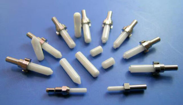
Ceramic feedthroughs serve as conduits for electrical signals, allowing them to pass through barriers such as vacuum chambers, pressure vessels, or hermetically sealed enclosures while maintaining a tight seal against moisture, gases, and other contaminants. This benefits makes ceramic feedthroughs essential in applications where need the reliability and durability.
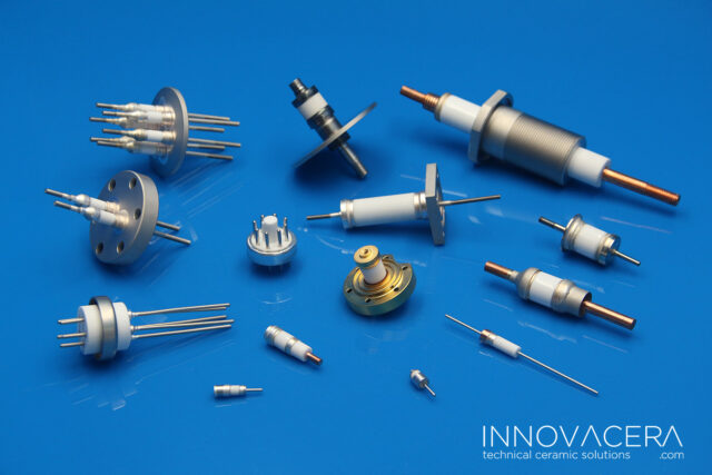
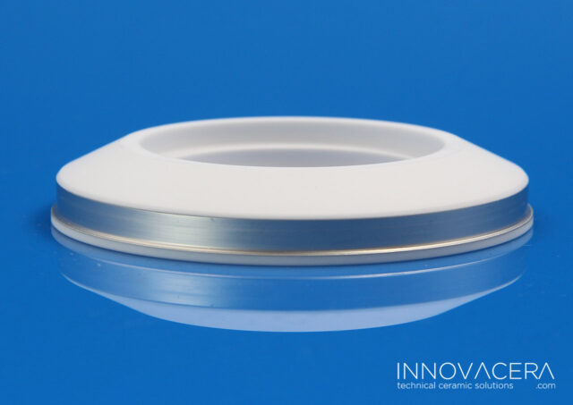
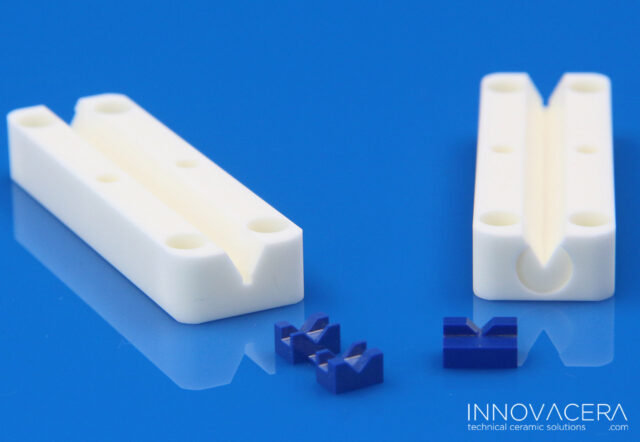
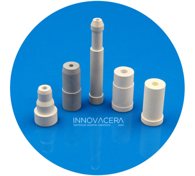
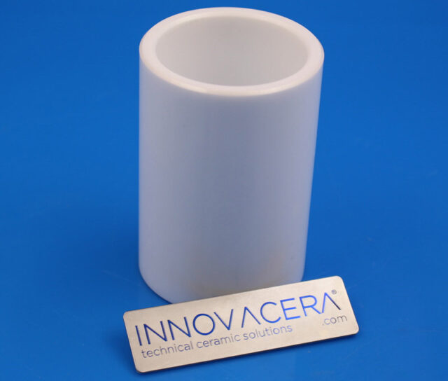
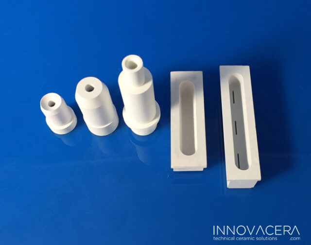
Innovacera ceramic-to-metal feedthroughs insulators are made by high purity alumina ceramics and Metals are made by stainless steel, nickel, copper, nickel-iron alloys, cupro-nickel alloys, molybdenum and Kovar. The braze materials Innovacera used are silver, copper, silver-copper, or gold-copper alloys. Innovacera controls and monitors critical processes of each ceramic feedthroughs, such as helium leak testing and x-ray measurements.
The ceramic feedthroughs have material properties such as high mechanical strength, thermal stability, and chemical resistance, making them ideal candidates for withstanding extreme operating conditions. Whether subjected to high temperatures, corrosive environments, or mechanical stress, ceramic feedthroughs maintain their integrity and functionality, ensuring long-term performance and reliability.
Even the slightest ingress of moisture or contaminants will effect the functionality of sensitive electronic components, so the hermetic sealing is critical. Ceramic feedthroughs provide an effective barrier against external influences, creating a reliable seal that prevents leakage and maintains the integrity of the enclosed environment. This is particularly crucial in industries such as aerospace, electrical and medical device.
Ceramic feedthroughs are excellent in providing electrical isolation between different environments or components within a system. By virtue of their dielectric properties, ceramics prevent the transmission of electrical currents, thereby ensuring that signals remain isolated and interference-free.
The versatility of ceramic feeders extends to a wide range of applications in a variety of industries. In aerospace, ceramic feedthroughs are used in satellite communications systems, spacecraft instrumentation and propulsion systems to provide reliable electrical isolation and sealing in the vacuum of space. In medical devices such as implantable pacemakers and defibrillators, ceramic feedthroughs can transmit electrical signals while maintaining a sterile and sealed environment within the device.
Additionally, ceramic feedthroughs also used for semiconductor manufacturing , where they help transmit electrical signals in vacuum chambers and plasma processing environments. Its rugged construction and high reliability make it an indispensable part for ensuring the integrity and performance of critical manufacturing processes.
If you need any ceramic to metal ceramic components such as ceramic feedthroughs, welcome to send your inquiry to us at sales@innovacera.com.
 Enquiry